Thermal management has long been a design challenge for power applications. When designs had space for large bulky heatsinks it was relatively easy to draw heat away from the circuit board and semiconductor components. However, as power levels and both power and circuit density have increased, this has become more difficult to handle. With today’s high-current, high-power applications and 650 V GaN power FETs, more efficient cooling of devices is often required or even mandatory. Here the additional performance offered by CCPAK’s top-side cooling is a must have.
When you look at the majority of power packages, one of the more obvious factors for thermal management is the conduction path they offer. For traditional SMD packages, heat tends to be dissipated through the bottom of the package, with the leadframe and PCB used as a heatsink. There is of course a limit to the amount of heat that can be taken out using the PCB. For improved efficiency of bottom-side cooled power MOSFETs, thermal ‘vias’ can be incorporated into the PCB to act as a pathway for heat energy to reach the main heatsink.

However, some applications need to be more thermally efficient or they need to reduce the heat being passed into the PCB. This is especially true for high-current / high-power applications such as power supplies for data centers, communication infrastructures, and automotive systems using FETs operating at 600 V or higher. With wide band gap devices, such as Nexperia’s 650 V GaN FETs, this becomes even more of a challenge given the higher power density and higher power dissipation they offer within a significantly smaller area. That is where top-side cooling offers a real performance boost. By thermally decoupling the printed circuit board and semiconductor, top-side cooling enables higher power density and/or longer system lifetimes.
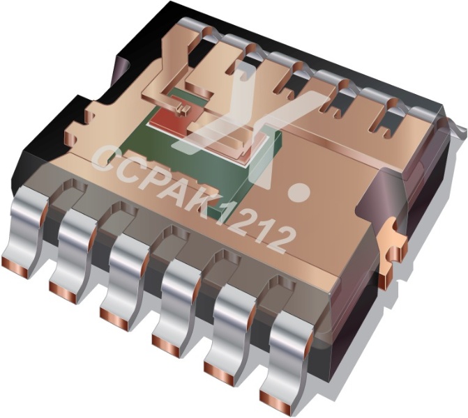
CCPAK1212i – a simple flip to top-side
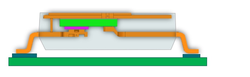
With the CCPAK development at Nexperia, we focused on bringing a suitable package footprint for our 650 V cascode-mode GaN HEMT devices. One of the key designs challenges was to make a connection between the HEMT gate and the FET source using our proven clip-bond technology. As I discussed in the blog, “CCPAK: copper clip comes to high voltage applications”, this was achieved by incorporating multiple internal pillars. As well as ensuring designers do not need to change the layout of their board (which would have been necessary with an external connection), these pillars provide a level of redundancy, improved thermal dissipation and spreading resistance.
The package design also makes it relatively straight forward to effectively flip the internal structure, so that the large, exposed copper clip HEMT gate / FET source is at the top of the package. This exposed copper clip can then efficiently dissipate heat away from the die and circuit board. For even higher current / higher power applications a heat spreader can also be attached via an isolated thermal pad.

So Nexperia’s 650 V GaN FETs in the top-side cooled CCPAK1212i enable the fast switching and higher efficiency in reduced size and weight, with a minimized total cost of ownership, yet at the same time offers designers of higher-current / higher-power designs with significant thermal management boost. In short, Nexperia managed to achieve a significantly higher power density with top side cooling devices compared to the bottom side cooled devices.
For more information on Nexperia’s range of CCPAK Power GaN FETs and to download datasheets, take a look at our CCPAK GaN FETs.