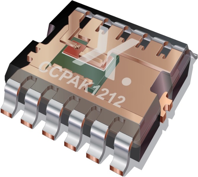
For some time the requirements of high-voltage applications have meant designers have had to rely on classic power packages such as TO-220 / TO-247 and D2PAK-7. However, as we move to ever higher switching frequencies, the limitations of these traditional packages become increasingly clear. Drawing on more than 20 years of experience using our proven copper clip technology, Nexperia has developed the CCPAK. Bringing all the recognized benefits of copper clip package technology to applications using 650 V and above.
From automotive electrification to highly efficient power supplies for data-centers and 5G communications, we are moving to a new era of fast switching, high-voltage power devices. To address this need we have seen bulk silicon devices fall by the wayside as new wide bandgap (WBG) semiconductors have become the new standard for applications using 650 V and above. However, while we have seen significant advances in terms of semiconductor devices, we have continued to house these components in classic power packages that were not designed for today’s applications.
Limitations of traditional packages
The TO-220 and TO-247 packages remain a mainstay in power electronics because they are proven, reliable power packages. These classic through-hole packages are more than capable of handling the voltage, current and heat dissipation of most high-power applications. And naturally they can easily be attached to a heatsink, ensuring excellent heat dissipation. A robust option for mid range switching frequencies, however the parasitic inductance caused by their long leads can be a limiting factor when it comes to high-frequency swithing.
Of course, with the D2PAK-7 there is a surface-mount package option for high-voltage power FETs. And just like the TO-220 this has become a proven workhorse of the industry. While parasitic inductance from long leads is no longer a concern, the D2PAK-7 does have internal wire bonds. And with mounting pressure on board space and height, along with the need to consider removing heat from the board and not just the power components, both the D2PAK-7 and TO-220 face significant challenges.
Package innovation to match technology advances
At Nexperia we realise that for some applications, traditional package options would be more than acceptable. But to really take advantage of the benefits of new high-voltage WBG semiconductors we would also need to develop a new package outline. To optimize the electrical and thermal performance, copper clip technology was the obvious choice especially given the results it has delivered to bipolar transistors, MOSFETs and rectifier diodes with our LFPAK and CFP package options.
Obviously the LFPAK88 was an excellent starting point for the development of a new high-voltage package option. In addition to the electrical and thermal benefits of copper clip, this delivers high board level reliability and advanced optical inspection (AOI) of joints compared with traditional through hole and QFN style packages. But to handle the operation of Nexperia’s GaN cascode mode FETs and to provide a future proof footprint, there were several features the new package would need to include.
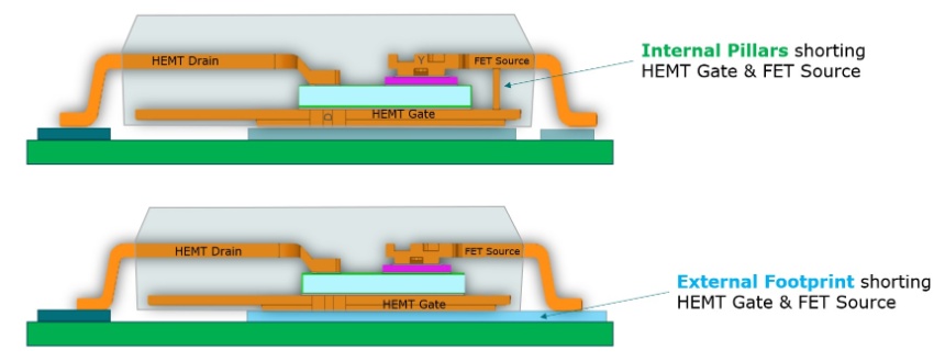
For example, with Nexperia’s 2nd generation H2 GaN technology we now have the HEMT gate on the bottom of the die. From a device perspective this improves dynamic RDS(on) and eliminates the floating substrate, while delivering more active cells with the same die size. As our devices are based on cascode architecture, we do need to make a connection between the HEMT gate and the FET source. This could be achieved via an external connection but would require designers to change the layout of their boards. So instead we have incorporated multiple internal pillars – this has the added benefit of providing a level of redundancy as well as improving thermal dissipation.


CCPAK1212: a new power package with proven heritage
One of more noticeable features of the new package is that it is a 12 x 12 outline. This still delivers a more compact (up to 10% smaller) footprint than the D2PAK-7, but importantly at only 2.5 mm it is almost half as high as the D2PAK-7. That means it is capable of housing future die sizes within the same outline, so as Nexperia expands its high-voltage portfolio, customers can benefit from designing with the same footprint.
In addition to bringing the benefits of copper clip to high-voltage power FETs, with the CCPAK1212i the package is effectively flipped. This enables top side cooling and gives customers the option to further enhance chip and board heat dissipation in hard switching topologies or where ambient temperatures can be an issue.

.jpg)
For more information on CCPAK and Nexperia's GaN FET portfolio join us at on July 2nd during the Nexperia Power Live. There’s both on-demand content and a dedicated live session for CCPAK.