Wide-bandgap (WBG) technologies such as SiC and GaN can deliver significant improvements in efficiency, power density and switching performance. Faster switching is what unlocks those gains, but it also narrows the margins for error. As switching speeds increase, the gate driver often becomes the key factor determining whether theoretical device performance can be translated into robust system operation.
Gate-drive design plays a critical role in managing switching behavior, mitigating unwanted transient effects and protecting power devices under fault conditions. With WBG devices it's a complex topic. For example, higher dV/dt increases susceptibility to Miller-induced turn-on; higher dI/dt magnifies the impact of circuit parasitics; and both push protection circuits to react faster than in a conventional silicon design. In this blog, we'll touch on a few practical gate-drive considerations for SiC and GaN devices.
Preventing unintended turn-on
A common design challenge for any FET is avoiding parasitic turn-on. One mechanism that can cause parasitic turn-on is charging gate-source capacitance (CGS) by displacement current in CGD, the Miller capacitance. During rapid drain-voltage transitions, CGS may present a lower impedance than the effective pull-down path of the driver circuit. This allows current through CGD to partially charge CGS, potentially causing the device to switch on unintentionally.
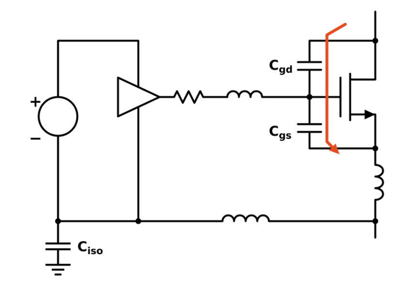
To assess susceptibility, designers should examine the ratio of gate-drain charge (QGD) to gate-source charge (QGS), or more specifically, QGS(th), the charge required to reach the threshold voltage. As a general design consideration, a ratio of less than one is preferable.
Devices with a lower QGD/QGS ratio are generally less susceptible to Miller-induced turn-on, while higher ratios typically require stronger gate pull-down capability, optimized gate resistance, active Miller clamps or negative gate bias. Using separate turn-on and turn-off gate resistors provides greater control over switching behavior. Where a gate driver has only a single output, a silicon Schottky diode can be used to create independent turn-on and turn-off current paths. However, particular care may be needed for devices with very low gate-threshold voltages – even the low forward voltage of a Schottky diode reduces margin.
Managing shoot-through and dead time
In half-bridge topologies, shoot-through (where the high-side and low-side switches conduct simultaneously) is one of the most critical failure modes to design against. Because SiC and GaN devices switch extremely quickly, careful dead-time management becomes increasingly important: insufficient dead time can create large current spikes, excessive losses and potentially destructive failures. Effective gate-drive design and timing help ensure safe switching while minimizing the efficiency penalty of adding dead time.
Isolation capacitance of the high-side drive
In high-side gate-drives, isolation capacitance associated with the floating power supply and signal path appears as a load on the switching node. This could be isolation capacitance of a transformer or isolated gate driver, or just the junction capacitance of a bootstrap diode – in fact any capacitance that gets charged and discharged with every switching cycle. The sum of such capacitances adds to loss in hard switching. Combined with parasitic inductance of the interconnect path, these capacitances also form resonant loads to the power FETs which may fall within their amplification bandwidth. Selecting transformers or bootstrap diodes with very low capacitance is therefore critical, as is the reduction of associated inductance in the path of transient currents.
Optimizing gate resistance and measuring gate behavior correctly
Selecting the lowest possible gate resistance does not necessarily produce the fastest or most efficient switching performance. In some cases, a small series gate resistance of several ohms reduces excitation of parasitic resonances, resulting in cleaner switching transitions that settle more quickly and generate lower overall losses. The optimum value is therefore often determined experimentally during system characterization.
Accurate gate-source voltage measurement
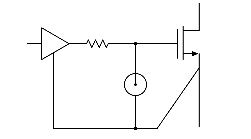
Gate ringing is a genuine concern in high-speed power converters, but the measurement technique is equally important. Long oscilloscope ground leads and poor probe placement can create apparent ringing that does not occur at the device itself. For accurate characterization, gate-source voltage (VGS) should ideally be measured using a high CMRR isolated probe referenced directly to the Kelvin source terminal, where available. Including an MMCX (Micro-Miniature Coaxial) connector in the PCB layout during the prototyping stage can significantly simplify troubleshooting (provided the placement and routing of the probe point do not introduce inductance in the measurement loop).
Avoid creating a common-gate amplifier
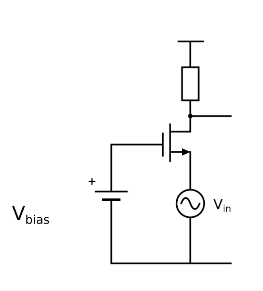
If there is gate ringing, don’t make the matter worse by amplifying it. If what appears at the gate is in fact ringing on the internal source inductance, which is transmitted to the gate by CGS, attempting to hold the externally measured VGS constant can effectively create a common-gate amplifier. In that case, it’s better to let CGS hold the on-chip VGS constant during the ringing transition, meaning the measured VGS will show ringing even though the on-chip VGS is constant. This is mainly an issue in packages with high common source inductance and no Kelvin Sense, such as the TO-247-3.
Gate-drive requirements vary significantly across WBG technologies
Enhancement-mode GaN
With narrow operating gate voltages of around 5 V to 6 V and maximum gate ratings of approximately 7 V, gate-voltage control is particularly important. In half-bridge topologies using bootstrap supplies, reverse-conduction events can potentially overcharge the bootstrap capacitor and increase gate voltage beyond safe limits. Appropriate clamping or block-out times should therefore be considered.
Cascode GaN
650 V high-power GaN devices can easily be driven with standard 10 V to 12 V gate-drive solutions. Note, however, that datasheets frequently recommend the use of a ferrite bead in the gate path to ensure stable switching behavior.
SiC MOSFETs
SiC MOSFETs typically require a higher positive gate voltage, with some applications using a negative turn-off bias for improved Miller immunity and a Kelvin source connection where available to minimize gate-loop effects.
Turning device potential into system performance
As adoption of GaN and SiC continues to grow, understanding how to control these devices (managing turn-on, dead time, isolation and gate ringing) is just as important as selecting the devices themselves. Gate-drive strategy, package technology and PCB layout all influence switching behavior, efficiency, EMI and long-term reliability. By addressing these elements together, designers can fully unlock the performance and efficiency advantages of WBG power devices.
For more on Nexperia’s WBG portfolio, check out our Wide-bandgap semiconductors Technology Hub.