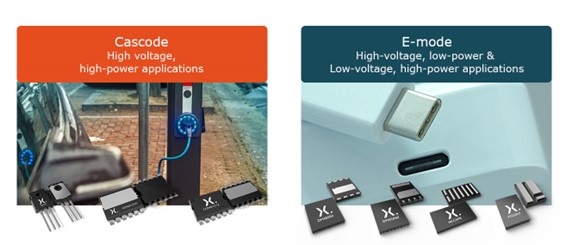
Power GaN FETs have become increasingly accepted since Nexperia first introduced our 650 V cascode devices at the end of 2019. In fact, according to Straits Research a market valuation of US$ 178.2 million in 2021 is expected to rise to around US$ 2.8 billion by 2030. By augmenting our 650 V cascode offering with high- (650 V) and low-voltage (100 / 150 V) e-mode (enhancement mode) devices, Nexperia provides designers with the optimum choice of efficiency and power density.
GaN technology delivers the best performance in power conversion topologies, and has proven its value in a range of demanding industrial automation, server, computing and telecom infrastructure applications. This in turn has led GaN to become less of a specialty technology and increasingly is being adopted into mainstream applications. This is because of all the wide bandgap (WBG) semiconductor materials, GaN offers the fastest transition / switching capability (highest dv/dt and di/dt) along with the best efficiency regardless of whether it is for low- or high-power applications. And Nexperia expects this transition to accelerate, as the commercial availability of e-mode devices helps drive the uptake of 48 V systems including the USB Power Delivery (USB-PD) Extended Power Range (EPR) mode.
Open the door to power and efficiency
While Nexperia’s cascode devices are clearly targeted at robust, high-power 650 V applications, our e-mode GaN FETs are suited to either low-power 650 V applications or high-power, 100 / 150 V applications. This is due to the inherent benefits that normally off enhancement mode technology offers. To start with these single die solutions offer very low gate charge (Qg) and output charge (QOSS), along with low RDS(on) values, to deliver outstanding switching.

That makes Nexperia e-mode GaN FETs ideal for a broad range of power conversion applications. They deliver optimum flexibility in AC/DC and DC/DC conversion, enhancing efficiency in fast, low-noise power supplies. That can be advantageous in everything from industrial automation installations to TV power supply units (PSU). In addition, photovoltaic (PV) micro inverters, fast chargers / adapters for e-mobility and USB-C power delivery also benefit from Nexperia’s e-mode GaN FET switching performance.
Beyond power supplies, e-mode GaN FETs bring performance and BoM (Bill of Materials) benefits. That can be in LED drivers for high-lumen output lighting installations or enabling higher torque and more power in BLDC / micro servo motors. While the low-noise performance and small footprint bring real value to non-automotive LiDAR applications and Class D audio amplification.
The right footprint
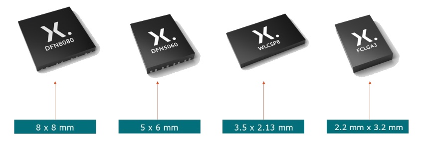
Many of the applications that our e-mode GaN FETs are targeting can be very space constrained. Therefore, to bring the highest power efficiency in the most compact solution meant choosing package outlines that would deliver on both requirements. For 650 V low-power applications that meant going with the industry standard Dual Flat No Lead (DFN) outline in standard 5 x 6 and 8 x 8 mm footprints. For the low-voltage, high-power devices, the decision was to use the 2.2 mm x 3.2 mm flip chip land gid array (FCLGA) for the 150 V device and the 3.5 mm x 2.13 mm wafer level chip-scale package (WLCSP) for the 100 V device.

To find out more about Nexperia’s e-mode GaN portfolio and to discover all the products, head over to nexperia.com/gan-fets.