Low dropout regulators (LDOs) offer a simple, cost-effective way to deliver high-quality power supplies. They are easy to use, but managing the heat the generate can be a challenge for designers. This blog explains why LDOs get hot, how power loss translates to junction temperature and how you can use thermal metrics to predict device behavior, design cooling solutions and determine safe operating limits in real-world applications.
Like other power devices, LDOs dissipate heat generated in the die through convection with the rate of dissipation governed by the thermal resistances in the system, principally the junction-to-ambient thermal resistance (RθJA). Heat is also dissipated via conduction through the sections of the package that are in direct contact with the circuit board.
Typically, heat sinks and forced-air cooling techniques are employed to reduce RθJA, which can impact system size and cost. Designers can also increase thermal performance by optimizing the layout of the PCB to improve the thermal interface and conduction cooling efficiency.
LDO power losses
The power dissipation in an LDO can be calculated quite straightforwardly - the input current (Iin) flow through one of two distinct paths: either through the pass transistor to the output terminal (Iout) or through the biasing circuitry to ground (Ignd).
The principle of power conservation states that the total input power equals the total output power. That means the power supplied to the LSO must be the sum of the power delivered to the load and the power dissipated within the LDO itself. Hence, we can express the power dissipated by the LDO (Ploss) as:
Take, for example, the NEX90530BPA-Q100 300 mA, 40 V LDO in the HTSSOP8 package. For this device, Iout = 300 mA. If we assume typical application values of Vin = 13.5 V and Vout = 5 V (± 1.5%) plus an ambient temperature of 25 °C, then we can read off Ignd from the graph in the product datasheet. In this case, Ignd = 1350 µA. Using the above equation, we can then calculate the maximum power loss in the LDO: Ploss = 13.5 V × (300 + 1.35) mA – 5.075 V × 300 mA = 2.545725 W.
Understanding thermal resistances
Nexperia provides detailed information on thermal resistance for all its products via datasheets. Thermal resistance is affected by many factors, including die size, die attachment, package, PCB layout and copper thickness. As a result, we usually determine thermal resistance through simulation, in accordance with the JEDEC standard.
As the figure below shows, chips have many thermal resistance parameters, some of which have a clear physical meaning. Of these, engineers most often use RθJA, RθJB and RθJC for thermal management.
Here we can see that heat is dissipated from the junction to the package case and the thermal resistance for this path is RθJC. Heat can also dissipate from the die to the PCB via the lead frame, die attachment and solder paste. The thermal resistance for this path is RθJB. Meanwhile RθJA represents a unified thermal resistance for the various heat transfer paths from the die to the air, including convection through the package, conduction via the PCB and radiation from exposed surfaces.
Estimating thermal resistance
The junction temperature can be calculated from a product’s thermal resistances. However, because thermal resistance depends strongly on the PCB, using the thermal resistances listed in the datasheet could cause inaccuracies as these are derived from simulation based on the JEDEC standard board. This is quite different from a system board. The datasheet values are intended to allow comparison of the thermal performance of different products.
In application, we usually determine the die-to-air thermal resistance RθJA on a case-by-case basis from the temperature difference and the power loss:
To demonstrate how to calculate RθJA, let’s again take the NEX90530BPA-Q100 as an example – this time as used in the Nexperia evaluation module (EVM).
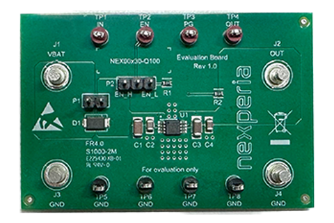
The EVM board has a two-layer design, measuring 60 x 40 mm with a standard copper thickness for internal layers (2 oz - ounces per square foot oz/ft² - or 70 µm thick). This gives a total heat dissipation area of about 3900 mm2. The thermal pad below the chip on the top layer is connected to the bottom layer through 5 vias to improve heat conduction.
For this calculation, let’s assume that voltage drop or load current is high enough for the device to just enter thermal shutdown. In other words, we can assume the junction temperature TJ = 175 °C. The temperature difference is then 175 °C minus room temperature (usually taken to be 25 °C) or 150 °C. The power loss can be calculated from equation (1). According to bench results, the NEX90530BPA-Q100 triggers thermal shutdown protection when VIN = 17.6 V with 300 mA load, while VOUT = 4.95 V. In which case, Ploss = 3.812 W.
Substituting these values into Equation 2, we see that RθJA = 39.35 W/°C. We can verify this result by retesting the thermal resistance according to JEDEC standard by using T3ster, giving RθJA = 38.9 W/°C which is close to our bench result.
Thermal resistance governs maximum load
We can now use this value of RθJA to estimate the device’s load capability at different temperatures. For example, imagine we want to determine the maximum load the NEX90530BPA-Q100 can take at TA = 125 °C. We can assume that TJ = 150 °C (the maximum operating junction temperature listed in the data sheet). The maximum power loss can then be calculated by rearranging equation 2, which gives a maximum power loss of 0.635 W. If VIN = 13.5 V, then IOUT_MAX ≈ 74.7 mA.
Estimating device temperatures in operation
Thermal resistance is not always the best parameter for calculating heat dissipation as the definition of thermal resistance is the temperature difference divided by the corresponding branch power. As figure 4 shows, the thermal resistance model can be represented as an equivalent circuit consisting of a heat source and thermal resistance.
The junction-to-top thermal characterization parameter, ΨJT, offers a better way to evaluate thermal performance. This quantifies the ratio of the difference in temperature between the junction and upper central surface of the package to the total power dissipated by the device:
We can use ΨJT to calculate the case temperature and then the junction temperature. Continuing with our example device, the NEX90530BPA-Q100, we assume TA = 25 °C, VIN = 13.5 V and IOUT = 300 mA. The measured value of VOUT is then 4.97 V. From Equation 1, we find that Ploss is 2.57 W. According to Equation 2, the difference between TJ and TA is 101.15 °C, which means TJ = 126.15 °C. Thermal imaging measurements (see Figure 5) show that TC ≈ 111 °C. Using Equation 4, we find that ΨJT = 5.89 W/°C.
It should be noted that ΨJT is highly affected by the board and environment, so we need to calibrate it based on the actual board. To do that we assume that TA = 25 °C, Vin = 15 V, VOUT = 4.96 V, IOUT = 300 mA. In this case, we calculate Ploss = 3.025 W and TJ = 144 °C. Then, for our previously calculated value of ΨJT, Equation 4 yields TC = 126.22 °C, which is consistent with the measurements in Figure 5.
The above shows how to calculate TC from ΨJT. However, if we can measure TC, we can use ΨJT to calculate TJ. Using the same values as above, if TC is measured to be 111 °C then we can calculate that Ploss = 2.57 W. Combining these values with our previously calculated ΨJT in Equation 4 gives TJ = 126.15 °C.
Using thermal characteristics in circuit design
RθJA and RθJC can be used in the initial stages of circuit design to predict junction temperatures and compare the thermal performance of different devices.
In practical applications, we need to measure and calculate the thermal resistance with the actual PCB used. RθJA can then be used to estimate the load capacity of a device. Finally, ΨJT allows you to calculate the case temperature of the device or, if the case temperature is measured, the junction temperature.