As power conversion systems continue to evolve, designers are under pressure to increase power density while maintaining efficiency and reliability. One of the most effective ways to achieve this is by increasing switching frequency, which can reduce the size of magnetic components and enable more compact system designs. However, higher switching frequencies place greater demands on the gate driver, making device selection increasingly important. Choosing the right gate driver can help designers improve power density without compromising robustness, efficiency or overall system performance.
Nexperia addresses these challenges with the NGD31251, a 28 V, 5 A dual-channel non-isolation low-side gate driver designed for silicon MOSFETs, IGBTs and cascode GaN devices. The device combines independent gate-drive channels with different timing sequences, fast switching performance and robust operation, enabling designers to support a range of power conversion topologies while maintaining efficiency and system reliability. An enable pin can also be used with external sensing circuitry to quickly disable the driver when required.
Balancing switching performance, robustness and flexibility
The device supports a wide supply voltage range from 4.5 V to 24 V and incorporates undervoltage lockout (UVLO) protection. This flexibility allows designers to optimize gate-drive voltages for different power technologies, including silicon MOSFETs operating at 12 V and IGBTs requiring drive voltages up to 18 V.
Offering a typical propagation delay of just 11 ns rising and 13 ns falling, together with support for output pulses as short as 10 ns, the NGD31251 enables switching frequencies of up to 1 MHz. Higher switching frequencies can help reduce the size of transformers, inductors and other magnetic components, contributing to more compact power conversion systems.
Power conversion systems can be susceptible to ground bounce and transient voltage conditions. The NGD31251 can tolerate input voltages down to -10 V, helping improve system robustness in applications where moderate ground bounce may be present. It also provides a typical peak source and sink drive current of 5 A per channel.
Optimized for demanding power conversion applications
With an operating junction temperature range of -40 °C to 140 °C, the NGD31251 is designed for demanding power applications. The device is available in both industry-standard SOP-8 and thermally enhanced bottom-side cooled MOSP-8 packages, with pinouts compatible with many existing gate-driver solutions.
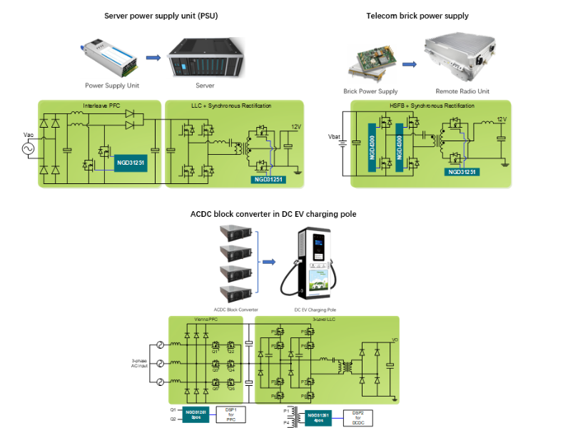
For applications that use multiple MOSFETs in parallel, such as high-current synchronous rectification stages in server power supplies, both output channels can be connected in parallel to deliver drive currents of up to 10 A. This approach can eliminate the need for additional totem-pole drive circuits, helping reduce BOM costs and PCB area.
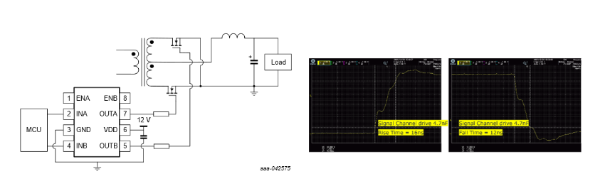
Typical applications include interleaved power factor correction (PFC), synchronous rectification in LLC converters and high-side power-device control when used with a signal transformer. End applications include server power supplies, telecom power modules, AC-DC converters for DC EV charging infrastructure, on-board chargers and DC-DC converters.