The structure of a small signal or medium power semiconductor device includes several subcomponents, each of which contributes to how it dissipates heat. In this blog, Nexperia defines the thermal parameters provided in its datasheets to enable designers to understand better how a semiconductor device's internal structure affects its overall thermal behaviour.
Package subcomponents that contribute to heat dissipation
Figure 1A shows the main subcomponents in the structure of a wire-bonded semiconductor device (such as a SOT23), including the lead frame, semiconductor die, bond wires and encapsulation. For high-power applications, bond wires are replaced by a frame connection (commonly called a clip-bond package), as shown in Figure 1B (such as a CFP3). Yet another class of device package includes extra terminals with a large surface area (a heat sink) to enable better heat dissipation from the device to its surrounding environment (Figure 1C, an example is a DFN2020D-3). Finally, for very high-temperature applications, a clip frame package combined with a heatsink can be used (Figure 1D, CFP15B is an example).

%20(1).2023-04-26-17-20-14.png)
%20(1).2023-04-26-17-19-54.png)
.2023-04-26-17-20-06.png)
.2023-05-08-14-28-16.png)
Understanding the meaning of thermal resistance
Thermal resistance can be considered the thermal equivalent of electrical resistance. This analogy can be helpful when designing for heat dissipation, and the thermal resistance between each subcomponent in a device must be considered. The thermal resistance R(X-Y) between two physical points is defined as the temperature difference ΔT(X-Y) between these points divided by the power P(X-Y) dissipated in the path between them as follows:
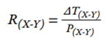
X and Y are reference points in the thermal system under investigation, and Nexperia typically considers point X as the junction of the semiconductor device (Tj ). Point Y is the solder point of the package or ambient temperature of the surrounding environment, as shown in Figure 2. The thermal resistances of Nexperia’s small signal devices are measured on standardised PCBs with different footprints. The results are shown on device datasheets as the Rth(j-a) values for different PCBs. These values are extracted using the Transient Dual Interface Method (TDIM), according to JESD51-14.

How Nexperia defines thermal parameters
The thermal resistances that exist between each of the subcomponents are defined as:
Junction to ambient Rth(j-a)
This is the overall thermal resistance of the system, including package, solder joints, PCB and optionally other components relevant to the thermal design.
Junction to solder point Rth(j-sp) or junction to mounting base Rth(j-mb)
This is the device’s thermal resistance when the reference point outside the package is the pin or package heatsink in the primary path for heat dissipation. The junction-to-mounting base resistance is mainly used for packages with a heatsink, while the junction-to-solder point is primarily used for smaller surface mount devices (SMD) or dual flat no-lead (DFN) packages.
Junction to top Rth(j-top) or junction to case Rth(j-c)
This is the thermal resistance of the minor heat dissipation path from the junction to the hottest spot on the top surface of the device. This parameter is not used nor accessible in real applications that do not employ top-side cooling.
Solder point to ambient Rth(sp-a)
This represents the thermal resistance of the entire system without the packaged device. The reference point is always the connection to the primary heat dissipation path of the device. In contrast, the ambient reference point is always the ambient air temperature (commonly 25°C or room temperature).
Coefficient junction to top Y(j-top)
This coefficient characterises the temperature difference from the junction to the hottest spot on the top surface of the device, correlating to the overall device power. By the strictest of definitions, this is not a thermal resistance since the temperature difference and power dissipation paths differ. Hence Nexperia denotes it using Y instead of R.
Summary
Manufacturers of semiconductor devices commonly include thermal resistance parameters in their datasheets, but their meaning is not clearly explained. In this article, Nexperia defined the thermal resistance parameters stated on its datasheets to help designers understand how subcomponents of a semiconductor device affect its overall thermal behaviour. For more information, please see Nexperia’s Diode Application Handbook.
To find space saving, thermal optimized and robust package solutions for the diodes and transistors in your next design, head over to our dedicated landing page: nexperia.com/save-pcb-space