In a previous blog, “When your switch choice is not a binary decision”, we touched on the basic principles and requirements of an analog switch when selecting from a host of different inputs. While these are relevant to all applications, from some specific applications some additional requirements that need to be considered. This is particularly the case with switching RF or audio signals and when multiplexing I²C signals.
When transmitting or switching analog signals, maintaining signal integrity is key. When analog signals are processed, they can be amplified, attenuated and delayed. Designers therefore need to find the right balance between these effects to assure safe operation of the respective application.
Some concrete effects can be:
- a drop in voltage due to high ohmic connection in a switch resulting in insufficient voltage level at the target device input
- a strong voltage overshoot right after switching resulting in damage to or unsafe operation of the connected device
- uncontrolled internal behavior caused by an absence of power supply combined with active inputs.
When constructing analog switches, there are various ways to configure the switched signal to match respective application requirements. For example:
- low ohmic analog channels – to achieve very low voltage losses in the signal path, pass transistors can be designed for low ohmic resistance (< 1 Ω). This can be achieved internally by expanding the channels of the pass transistors, but is associated with higher channel capacitance which can cause switching transients
- limited voltage overshoot – dedicated control circuits in the switch can be implemented to prevent overshoots in combination with fast switching
- power down mode – active inputs should not cause unwanted behavior such as wake-up or VCC being driven by active signals connected at the output, resulting in a need for power-off protection.
Characteristic behavior and features of analog switches
Various functions and features can be built into an analog switch to optimize its behavior with respect to dedicated requirements. For example, consider a switch that is in front of a subsystem IC, where the switch is controlled by a microcontroller. In a power-up phase, the switch and the subsystem are still in power-off mode, whereas the microprocessor which is driving the digital input signal of the switch, is already active.
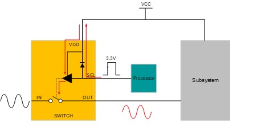
Naturally it is important to avoid the unwanted wake-up of the subsystem via the digital input of the switch and its internal ESD clamp diode. The preventive mechanism is called fail-safe logic. Internal circuitry prevents the connection of the input to the VCC supply pin while the device is powered down. The scenario is shown in Figure 1.
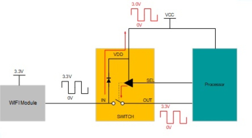
A similar effect can occur when the connected input device is powering the VCC supply of the switch via its analog input pin. The mitigating effect for this is called power-off protection and is shown in Figure 2.
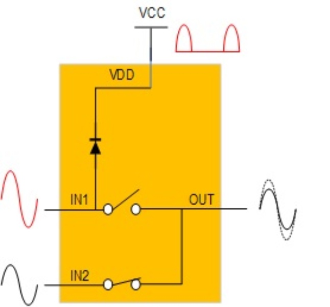
Another important aspect of analog signal switching quality can be found in the behavior of analog multiplexers, where one of several analog inputs is selected and connected to the analog output. The internal circuit construction for mitigating channel current injection is shown in Figure 3 and was touched on in the previous blog, “When your switch choice is not a binary decision”.
Related application examples
RF signal switching
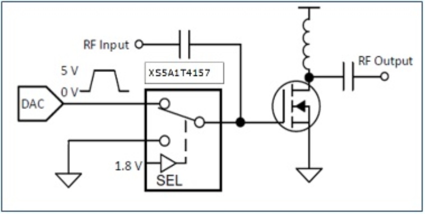
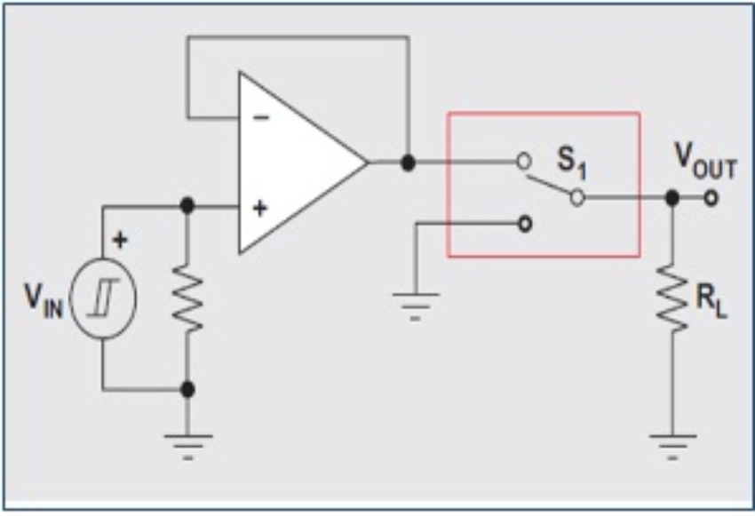
When switching RF signals, signal integrity is important as frequencies are high and the signal is vulnerable. In the example below, an RF input signal is added to a DAC output or switched to GND. The resulting signal is driving y MOSFET which is controlling an RF output signal. Due to the high frequency of the RF signal, any switching transients of the switch would disturb the RF output signal, thus any over- or undershoot behavior of the switch must be suppressed. In this example, the low-ohmic single-pole double-throw analog switch (SPDT) XS5A1T4157 from Nexperia assures precise switching without overshoot, making it the ideal solution for this application case.
Switching Audio signals
High quality audio signals can only be delivered if the full voltage amplitude is transmitted. Any losses in the signal path can distort the signal quality and reduce the bandwidth. Therefore, if a signal needs to be switched the switch must be as low ohmic as possible. Non-selected signal paths of the switch must have a high impedance in order to avoid cross-talk effects. The example illustrated in Figure 5 shows a switch used to turn the headphones of an audio system either on or off. As the switch is only used for on/off switching and remains static during operation it is only required to be low ohmic and not necessarily have low overshoot. Nexperia’ s solution for this scenario could be the low-ohmic SPDT analog switch XS3A1T3157 with and Ron value of typically 0.5 Ω, ensuring very low voltage drop.
Multiplexing I²C signals
I²C is an open drain bus protocol. While the high level is generated via pull-up sources and resistors, which are permanently active, participants can actively pull down the voltage levels of the clock and the data signal. That means they need to pull down the voltage to a low level against the pull-up circuit, in particular the pull-up circuit at the receiver side. And the receiver at the other end of the transmission line needs to recognize the low level. A common issue of I²C transmissions over a longer transmission line is the voltage drop over the line. If it is too high, the receiver voltage is not low enough to be recognized as low. Therefore, transmission lines and switching devices in I²C networks must be low ohmic.
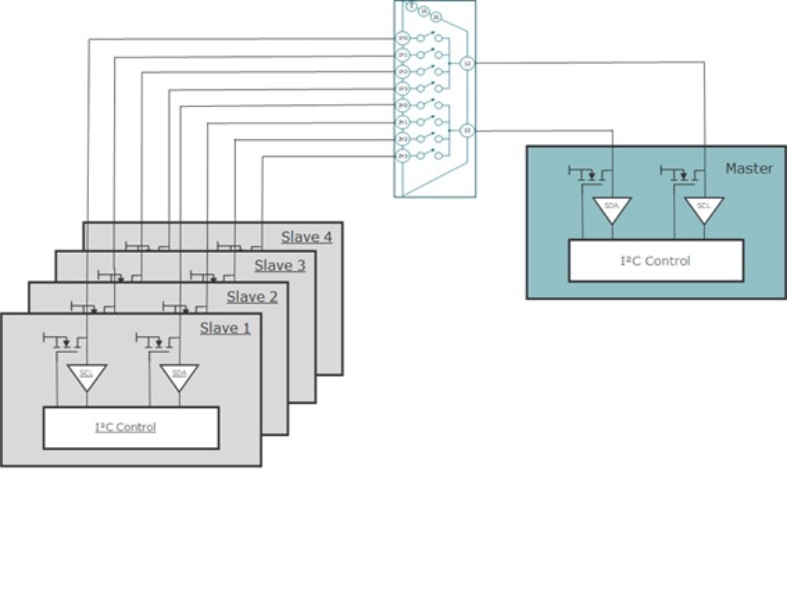
A possible I²C network configuration as shown in Figure 6 uses an analog switch to split between four target devices. This is needed if target devices have the same I²C address or the address range is limited. Two additional selection signals are needed to select the channel and an enable pin can be used to enable or disable the device. Due to the low ohmic channel connection of < 1 Ω, the switch has does not affect the signal integrity on the I²C bus.