In today’s electronic devices, the processing of information and data lies purely in the digital domain. However, analog signals continue to play a vital role when it comes to interfacing with the real world. With the multitude of sensors measuring the data points we need in today’s ‘smart’ world, many devices need to select from a host of different inputs. But knowing which analog switch to choose, and what parameters are important, is increasingly a challenge designers are facing.
To meet our information demands, data needs to be fast and accurate. The progress in sensor technology, particularly in terms of miniaturization, is helping increase the availability of simple cost-effective sensing. In fact, as well as being a useful enhancement in many control units, sensing environmental attributes such as temperature, humidity, brightness, etc. is an increasingly popular feature in many consumer applications. In complex electronic systems, the result has been a dramatic rise in the number of analog signals that need to be processed.
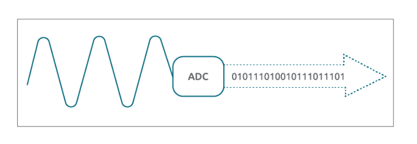
Wherever physical properties are sensed or measured, the primary resulting electrical signal has a continuous voltage level within defined limits. This then needs to be converted into a digital signal that can then be processed by the system. In most applications, analog-to-digital (AD) conversion is done with signals operating at moderate frequencies. An analog switch can be used to expand the number of channels and switch between them allowing the converter to process one of the channels within a given time slice. Therefore, for high performing systems, various parameters of both the AD-converter and the analog switch need to be considered.
The basic principles
In most data conversion applications, resolution and the accuracy are very important parameters. Resolution is determined by the number of bits, so 10 bits results in 210 or 1024 different digital levels. Accuracy is the deviation of the sampled level due to a source of error such as a voltage drop in the signal path or a disturbing side channel effect that alters the voltage level of the signal. For accurate AD conversion it is therefore vital to have good signal integrity.

Of course, this applies not just to the converter, but any switch in front of the converter. Signal integrity requirements can be met by the switch if it is sufficiently low ohmic to allow high accuracy. However, it must also have a low capacitive to keep switching transients under control. Unfortunately, to achieve low ohmic characteristics tends to come at the expense of increased capacitance. So, getting the right balance is key.
Requirements of the switch
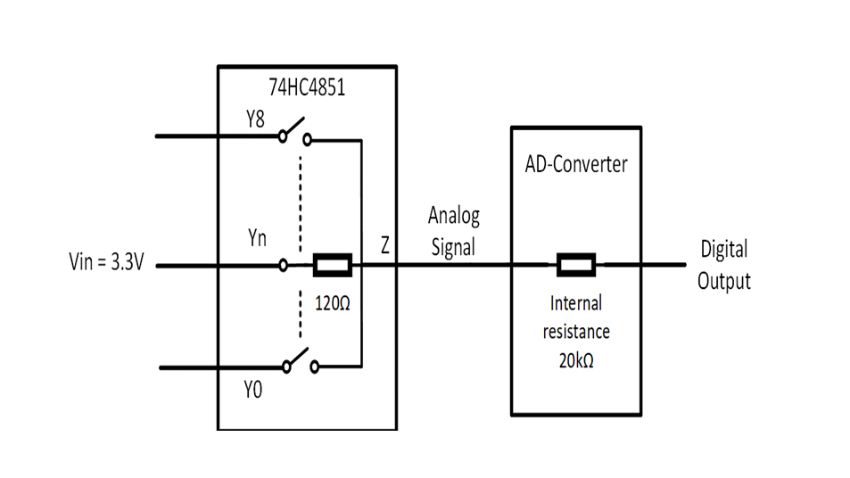
The allowed channel resistance of the switch can be derived by the accuracy requirement and the internal resistance of the AD converter. In the figure below, a typical AD-converter and 8:1 Multiplexer is shown. For a calculation of the allowed Ron resistance of the analog switch we can consider the following application scenario: the lowest internal resistance of the AD converter is 20 kOhm. For a given maximum input volage per channel of 3.3 V, the voltage drop in the channel of the switch is:
VSW = (Vin / (Rsw + RAD)) * RSW = (3.3 V / (120 Ω + 20000 Ω)) * 120 Ω = 19.68 mV
This voltage drop means a constant offset for the conversion. It can be related to a common 10-bit resolution: 3.3 V / 210 = 3.22 mV, which is approximately related to 6 Least Significant Bit (LSB) of 19.68 mV. The constant voltage drop factor can be either corrected by software in the system or is accepted within the accuracy requirements. Thus the requirement of the inner resistance of the switch is to be constant rather than extremely low.


Channel current injection protection
Another important aspect and source for signal disturbance is the switching behaviour between channels. Channel capacitances can induce transient voltages if capacitances are too high. They are kept low in the design at the expense of the channel resistance.
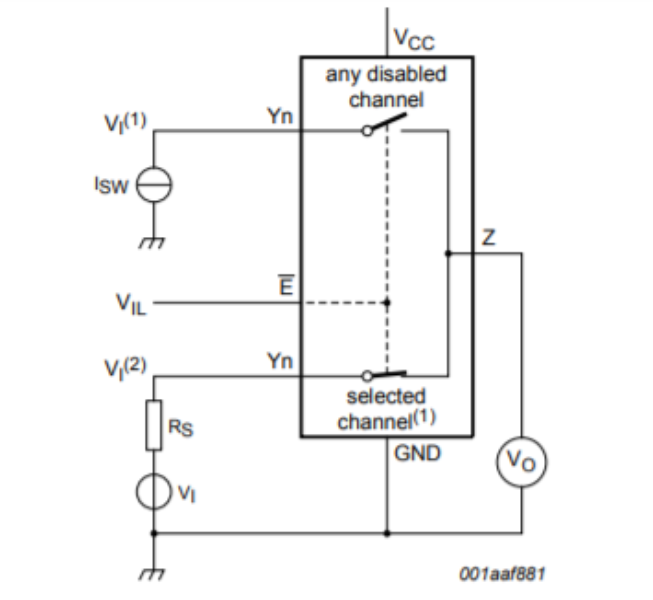
Under ‘normal’ conditions or behaviour, while only one of the 8 channels is selected at any time in an 8:1 Multiplexer, all channels are continuously under power and have a certain voltage level. However no current flows into the switch (except low leakage current) from the channels are switched off.
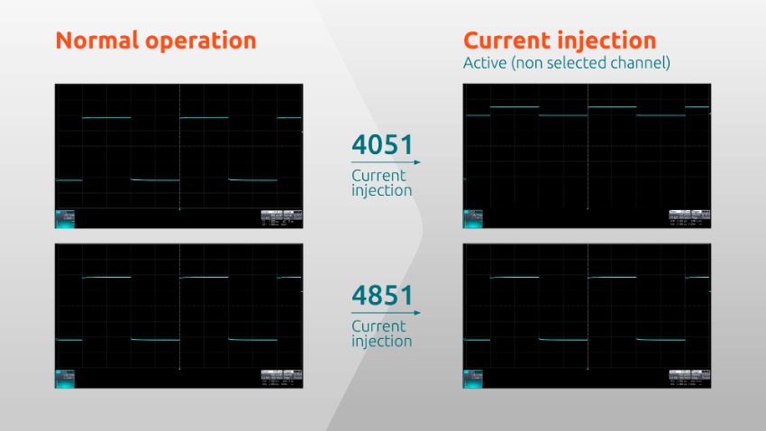
In certain situations, the input voltage of a non-selected channel might be increased, even higher than the VCC level of the switch, perhaps only for a short time frame. In a standard design construction, this exceeded input voltage would also affect the output voltage as it lifts the output level via VCC. As a result, the voltage of the selected channel is manipulated, impacting the result of the AD-conversion. The mitigation mechanism against this effect is the current injection control feature, which Nexperia includes on the 4851 family of 8-channel analog multiplexer/demultiplexer. This -ensures a clear differentiation between high and low values.
