By eliminating internal bond wires and reducing source lead length, Nexperia’s LFPAK88 minimizes parasitic source inductance created during switching, resulting in greater efficiency. While alternatives like leadless (QFN) packages or utilizing a Kelvin source connection can offer similar benefits they also have significant drawbacks, making the LFPAK88 the winner with ‘the shortest path to higher efficiency’.
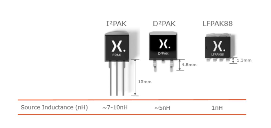
One factor that makes a difference to MOSFET efficiency is parasitic source inductance. This is created in the source leads and bond wires during every switching event. As a rough rule of thumb: every 1 mm of source path generates 1 nH of source inductance. So, by minimizing the inductance we can improve switching efficiency.
In older leaded packages, such as the I²PAK (SOT226) and D²PAK (SOT404) the combination of long source leads and internal bond wires increases source inductance. However, by replacing the internal bond wires with a copper clip and minimizing source lead length, the LFPAK88 significantly reduces the source inductance. It achieves this without sacrificing temperature cycling and soldering reliability, which are among the drawbacks of alternative options like leadless (QFN) packages or utilizing a Kelvin source connection.

A quick fix?
If we really want to minimize source inductance, why not just remove the external leads altogether? QFN type packages take this approach, using connections underneath the package to affix directly to the PCB. This does lower parasitic source inductance but creates a series of other issues in its place – such as soldering, solder inspection and surviving application temperature cycling (board level reliability) which are overcome by the short external gull wing leads of the LFPAK. Furthermore some QFN packages remove the leads to reduce inductance but have internal bond wires which add it back in.
Does a fourth pin really speed things up?
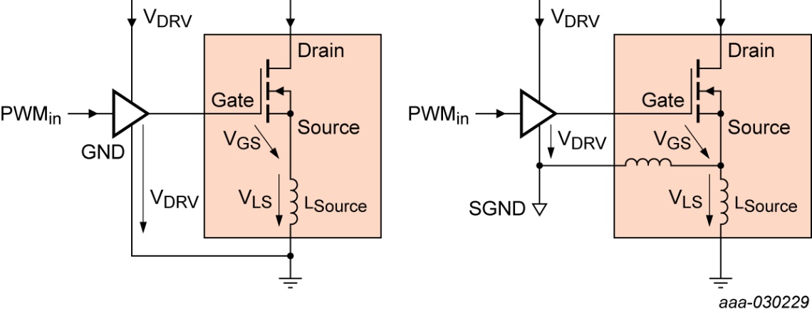
Another recent concept to remove the effect of parasitic source inductance is employing a Kelvin source connection. This technique adds a fourth pin to the usual 3-pin configuration to separate the power path from the path of the driving signal. Of course it is more commonly associated with fast switching, high-voltage, high-current devices (such as Silicon Carbide) for high power (> 1 kW) SMPS in conventional leaded packages with larger source inductances to overcome (10-20 nH).
Although the source inductance still exists, the Kelvin source pin breaks the feedback loop to the gate pin, thereby negating the negative effects of the source inductance. However the best results are found in higher voltages (> 500 V) and high current.

Nexperia investigated whether adding a Kelvin connection would be beneficial. While a fourth pin obviously can be advantageous, at lower voltages (≤ 100 V) and with the very low source inductance of the LFPAK88, the resulting benefit was minimal. Certainly not enough to counter the need for more complicated driving circuitry or the reduction in maximum current capability.
LFPAK offers more benefits than conventional packages
The combination of short external leads and copper clip enable minimal parasitic source inductance for LFPAK88, whilst still retaining temperature cycling and soldering reliability compared to leadless QFN packages. Specifically for driving traditional automotive motors / pumps etc. with ≤ 100 V MOSFETs, the addition of a Kelvin source pin inside the LFPAK88 package offers no clear benefits. So while alternatives like QFN and the Kelvin source connection can deliver a reduction in parasitic source inductance their drawbacks mean they cannot offer the same overall benefits of the LFPAK88, making LFPAK the clear winner with ‘the shorter path to higher efficiency’.