Silicon Carbide (SiC) has many advantages over silicon in high-power applications, including higher operating temperature and more efficient switching at high frequencies. However, compared to silicon fast recovery diodes, some characteristics of the pure SiC Schottky diode can still be improved. This blog shows how Nexperia has combined an advanced device structure with innovative process technology to bring SiC Schottky diode performance to the next level.
Merged-Pin Schottky (MPS) structure lowers leakage currents
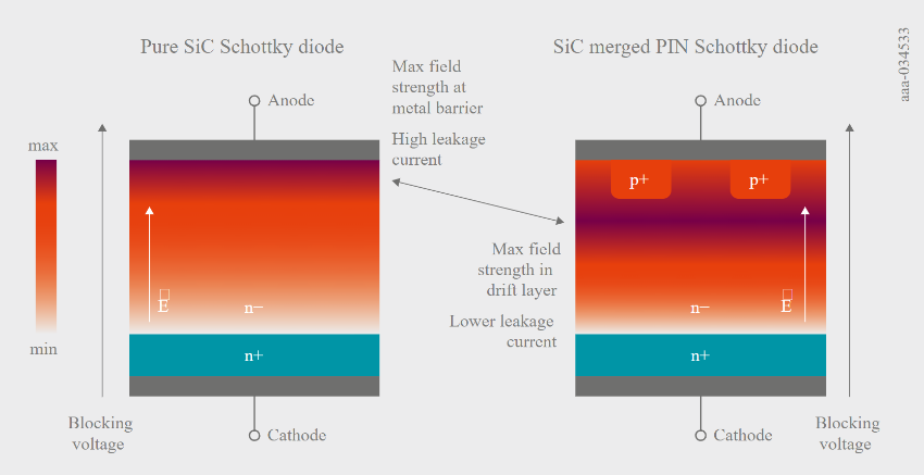
Imperfections at the metal-semiconductor interface are responsible for leakage currents in SiC Schottky diodes. While these can be reduced by using a thicker drift layer, it comes with the disadvantage of higher ohmic and thermal resistance, which is disadvantageous in power applications. Therefore, Nexperia SiC developed their SiC diodes as hybrid device structures, shown in Figure 1, to overcome these issues. This ‘merged PiN Schottky’ (MPS) effectively combines a Schottky diode and a P-N diode connected in parallel.

P-doped areas are implanted in the drift zone of a conventional Schottky structure, forming a P-ohmic contact with the metal at the Schottky anode and a P-N junction with the lightly-doped SiC drift or epi-layer. Under reverse bias, the P-wells ‘push’ the general area of maximum field strength downwards into the almost defect-free drift layer, away from the metal barrier with its imperfections, reducing the overall leakage current, as shown in Figure 1. The P-wells' physical placement and area (compared with the size of the Schottky diode) and doping concentration affect the end characteristics, with forward voltage drop traded against leakage and surge currents. As a result, an MPS device can operate at a higher breakdown voltage with the same leakage current and drift layer thickness.

MPS diodes exhibit better surge current robustness
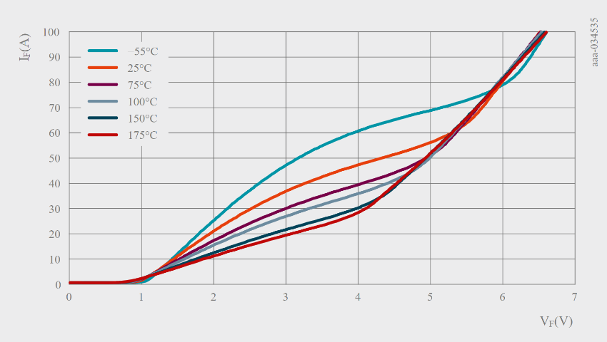
The surge current performance of SiC devices relates to their unipolar nature and relatively high drift layer resistance, and the MPS structure can also improve this parameter. The reason for this is that the differential resistance of a bipolar device is lower than that of a unipolar type. Under nominal operation, the Schottky part of the MPS diode conducts almost the entire current to effectively behave like a Schottky diode, delivering the same benefits during switching. During high transient surge current events, the voltage across the MPS diode increases beyond the built-in P-N diode cut-in voltage, which begins to conduct with lower differential resistance. This diverts current, limiting dissipated power and relieving the MPS diode from thermal stress. Without the P-N diode, the Schottky diode alone would have to be significantly over-dimensioned to allow for transient over-current events in the target application. Parts could be paralleled (or extra circuitry added) to limit over current, but this would increase costs. Here again, the dimensions and doping of the P-wells create a trade-off between forward voltage drop (in regular operation) and surge withstand capability. The best choice depends on the application, and Nexperia offers diodes to suit a wide range of hard- and soft-switching applications.
MPS diode reverse recovery characteristics
Besides their improved static behaviour, SiC MPS diodes also offer benefits during dynamic switching operation. One significant advantage over silicon-based P-N diodes relates to reverse recovery behaviour. The reverse recovery charge is one of the main contributors to power loss in silicon fast recovery diodes, adversely affecting converter efficiency. Several parameters affect this, including diode turn-off currents and junction temperatures. In contrast, only majority carriers contribute to the overall current flow in SiC diodes, meaning they exhibit almost constant behaviour, with little of the non-linear performance of silicon fast recovery diodes. Hence, it is easier for power designers to predict their behaviour because they do not need to consider various ambient temperatures and load conditions.
Innovative ‘Thin SiC’ diode structure further enhances MPS diode performance
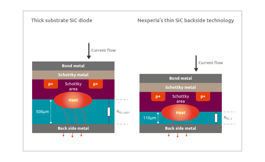
Nexperia’s MPS diode provides additional advantages derived from reduced die thickness during fabrication. The unprocessed SiC substrate is N-doped, and SiC epitaxial layers are grown to form the drift region. The substrate starts with a thickness of up to 500 µm, but after epitaxy, this adds unnecessary electrical and thermal resistance in the current and heat-flow path to the back-side metal. This increases forward voltage drop and junction temperature for a given amount of current. Nexperia’s solution to overcoming this is to ‘thin’ the underside of the substrate by grinding it. Material quality and grinding precision are crucial during this process step to avoid non-uniformities and consequent performance degradation of the diode (which could result in devices failing in the field). Furthermore, advanced manufacturing expertise is required because of the hardness of SiC (9.2 to 9.3 on the Mohs scale, compared to 6.5 for silicon). Figure 3 shows the effects of the process, with Nexperia’s ‘thin SiC’ technology achieving a reduction to about one-third of the original substrate thickness.

As a result, the thermal resistance from the junction to the back-side metal is dramatically reduced, resulting in lower device operating temperature, higher reliability (due to improved surge current robustness) and lower forward voltage drop.
Summary
The number and types of available SiC Schottky diodes continue to increase, including devices with a conventional structure and those with a more advanced MPS structure. Nexperia has combined the advantages of a wide bandgap semiconductor material (silicon carbide) with an MPS device structure and additional benefits derived from its “thin SiC” technology in its new SiC Schottky diode. Drawing on its expertise in process development and device fabrication has enabled Nexperia to push the performance of this new product offering to a level that places it firmly in the top tier of SiC diodes on the market today.
To find out more about Nexperia’s Silicon Carbide Schottky Diodes portfolio and to discover all the products, head over to nexperia.com/sic.