The world needs change makers and Nexperia’s latest introduction of side-wettable flanks (SWF) on a 5-pin package for logic functions is set to be a very positive disruptor. A wide variety of functions across voltage families such as HC, AHC, LV, LVC, AUP have recently been added in Nexperia’s new SOT8065 (XSON5) package, known as the GZ family. This compact package delivers improvements in product quality, reliability, and production cost, while supporting the ongoing trend toward smaller, more efficient applications.
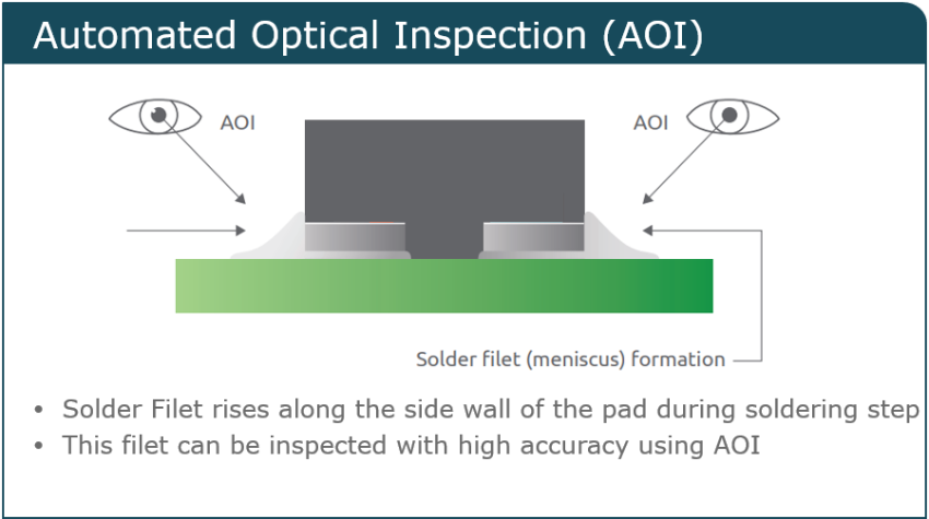
As electronic devices continue to shrink, manufacturing challenges become more pronounced – especially around quality assurance. Once an integrated circuit (IC) package has been soldered onto the printed circuit board (PCB), the quality of the solder bond must be checked to ensure the IC is reliably mounted and fixed (reducing potential failure during the product lifetime). In traditional leaded packages, solder joints are visible and can be easily inspected using automated optical inspection (AOI) systems. Leadless packages, however, hide these joints beneath the component, requiring costly X-ray equipment to verify solder integrity.
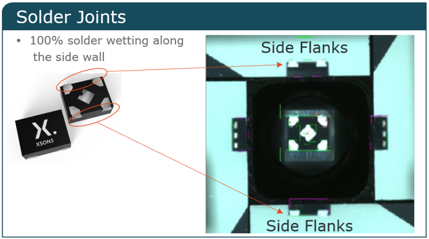
The obvious solution to this challenge is to make the solder contact visible on leadless packages. Nexperia has achieved exactly that by extending the solder pads of the SOT8065 (XSON5) package along the edge of the package. When these packages are soldered onto the PCB, the solder forms a fillet that extends along the edge of the pad. Simple inexpensive cameras can easily detect the solder fillet and can be used for quality inspection in the production lines. This approach has already proven effective in Nexperia’s diode and transistor portfolios, and now with the SOT8065 brings the same benefit to logic functions.


Better quality at an even better price
Possibly the key benefit of the SOT8065 is that it brings the cost of quality assurance for leadless packages in line with that of leaded packages. Quality assurance is critical for several applications, particularly in automotive, where the SOT8065 is ideal. When compared to other leadless packages without side wettable flanks, this package has the added advantage of stronger solder bonds that are more resistant to shear stress. In addition, with a smaller footprint compared to leaded packages, this package enables a high IC board density, reducing board size and helping deliver a lower overall cost of the application.
Subtle features that delight designers
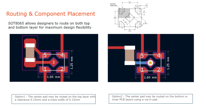
This latest micro-logic package has been designed with attention to the finer details. Routing the center pad on previous generation of leadless packages could be a challenge as the pad-to-pad distance was narrow, leaving very little clearance for the trace. The alternative route required a via under the pad, which is an expensive step. By offering a large pad-to-pad clearance of 0.45 mm, the SOT8065 allows a trace width and clearance of 0.15 mm. And with an enlarged center pad and unique design that allows the IC to auto align to the solder footprint during the soldering step, soldering this leadless package is no longer an engineering challenge and that requires a fine hand. It is these subtle yet impactful design enhancements that make the SOT8065 the go-to-package for engineers.

Creating elegant products at competitive prices
For applications where space is at a premium, this package offers a practical path to more elegant, efficient designs. With up to 75% PCB area savings compared to equivalent leaded packages, the SOT8065 allows engineers to create compact designs without sacrificing performance. The internal die remains consistent with leaded versions, ensuring familiar electrical behavior while reducing board space.
It meets RoHS requirements, features a dark green molding compound, and carries a high moisture resistance rating of MSL1. Its uniform 7 μm tin coating on side and bottom pads enhances reliability in harsh environments, and the package is fully free of delamination, aligned with Nexperia’s focus on durability and long-term performance.
As designs become ever more complex, the relative cost of PCB real estate can be a be a real deal breaker especially when it comes to space constrained applications. Leadless packages with side-wettable flanks like the SOT8065 allow designers to build elegant products without worrying about how they will fit everything into the given size. Freeing them up to be more creative and design without constraints.