Meeting the heat dissipation requirements for an application requires designers to compare and contrast the thermal behaviour of different semiconductor package types. In this blog, Nexperia discusses the heat dissipation pathways in its wire-bonded and clip-bonded packages so designers can decide the most appropriate choice.
How heat flows in a wire-bonded device
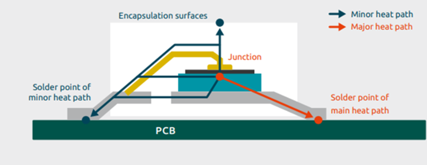
The primary pathway for heat flow in a wire-bonded device is from the reference point junction to the solder point on the printed circuit board (PCB), as shown in Figure 1. To a first-order approximation, the contribution of the minor power dissipation pathways (also shown) is negligible in thermal resistance calculations.

Dual heat flow pathways in a clip-bonded device
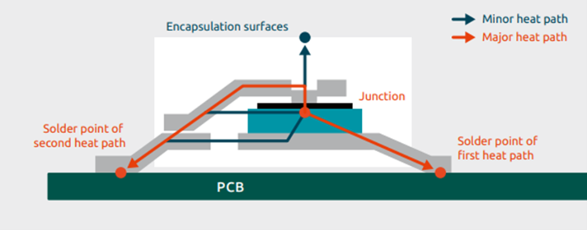
Clip bond packages differ thermally from wire-bonded packages in that heat dissipated from the junction of a device can follow two different paths - heat travels through the lead frame (as with wire-bonded packages) and the clip frame.

Two reference solder points complicate the definition of thermal resistance at the junction-to-solder point—Rth(j-sp). Since these may not even be at the same temperature, thermal resistance becomes a parallel network.
Nexperia uses the same approach to extract the Rth(j-sp) value for clip-bonded and wire-bonded devices. The value characterises the main dissipation path from the die to the lead frame to the solder point, making the values for clip-bonded devices comparable to wire-bonded devices in a similar PCB layout. However, the overall heat-dissipation potential of a device is typically higher since the second path is not used to its full extent when extracting the value for Rth(j-sp).
The fact that there is a second significant dissipation pathway creates opportunities for improved PCB design. For example, with wire-bonded devices, the only option is to remove heat via a single path (most via the cathode pin in the case of a diode); both terminals can be used with clip-bonded devices.
Simulating the thermal performance of semiconductor devices
Simulations demonstrate significantly improved thermal performance with thermal pathways for all device terminals on a PCB. For example, 35% of the heat dissipated in a CFP5 (Figure 3) packaged PMEG6030ELP diode transfers via the copper clip into the anode pin, while 65% dissipates through the lead frame into the cathode pin.

Figure 3. CFP5 packaged diode
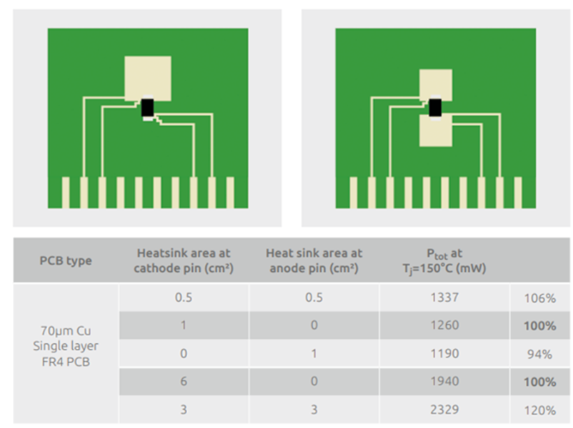
Simulations also show that splitting the heatsink between both terminals (as shown in Figure 4) is advantageous to heat dissipation.
If a 1cm² heatsink is split into two 0.5cm² heatsinks beneath both terminals, the power that can be dissipated by the diode at the same temperature increases by 6%.
Two 3cm² heatsinks allow for approximately 20% more power dissipation than with a standard design and a 6cm² heatsink at only the cathode.

Nexperia helps designers choose the best package for their application
Some semiconductor device manufacturers do not provide designers with the information they need to determine which package type can offer the best thermal performance for an application. In this article, Nexperia described the heat dissipation pathways in its wire-bonded and clip-bonded devices so designers can make the best choice for their applications. For more information, please see Nexperia’s Diode Application Handbook.
To find space saving, thermal optimized and robust package solutions for the diodes and transistors in your next design, head over to our dedicated landing page: nexperia.com/save-pcb-space