Some of the key drivers behind the growing popularity of Silicon Carbide (SiC) MOSFETs include the growing demand for higher efficiency, lower energy consumption and reduced total cost of ownership in modern power electronic applications such as charging stations, solar photovoltaic (PV), electric vehicles (EV) drives, uninterruptible power supplies (UPS) and battery energy storage systems (BESS). This blog article looks at some of the unique features of Nexperia’s SiC MOSFET devices which bring advantages to these applications that similar devices from other manufacturers simply cannot deliver.
Advantage No. 1: Lowest drift in RDSon over operating temperature range
In general, SiC is renowned for its temperature stability, however, as the junction in a typical device heats up, RDSon typically increases by a factor of between 1.6 and 2 across the full operating temperature range. For example, a device with RDSon = 40 mΩ at 25 °C can have RDSon= 80 mΩ when the junction temperature reaches 175 °C. Nexperia has addressed this limitation by designing its 1200 V SiC MOSFETs to have the industry’s lowest RDSon temperature drift – a factor of only 1.4 (Figure 1). This means that a Nexperia SiC MOSFET with RDSon = 40 mΩ at 25 °C will see this value increase to only 56 mΩ at a junction temperature of 175 °C. This superior temperature stability has the benefit of reducing conduction losses at high operating temperatures compared to similarly rated devices from other vendors. This feature makes Nexperia SiC devices ideal for demanding power conversion applications which commonly experience elevated operating temperatures such as motor drives, charging infrastructure, solar PV, UPS and others.

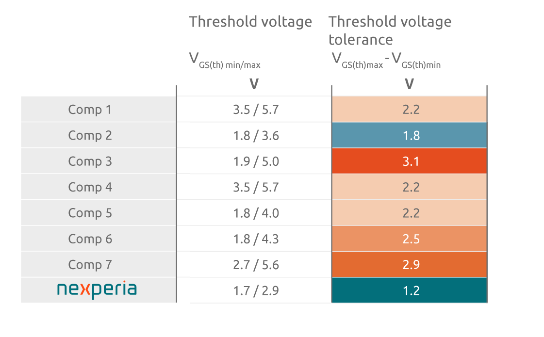
Advantage No. 2: Lowest threshold voltage tolerance
The threshold voltage (Vth) for a MOSFET is an important indicator in safe device operation, with values in the range of 2.5 to 4 V usually offering an acceptable operating margin. Nexperia has designed its 1200 V SiC MOSFETs to have a threshold voltage of 2.9, comfortably within this safe operating range. However, while the actual value of threshold voltage is important, a related key parameter for safe device operation is threshold voltage tolerance. This parameter represents the variation between the specified minimum and maximum values of threshold voltage. A key advantage of low threshold voltage tolerance is that it enables highly symmetrical switching behaviour between multiple SiC MOSFETs connected in parallel, a common arrangement in many power applications. This ‘balanced parallelization’ reduces the stress on individual devices (which might otherwise experience high current loads during dynamic switching operation), enhances circuit performance and extends product lifetimes. Compared to similar competing devices, Nexperia’s SiC MOSFETs exhibit the lowest variation in threshold voltage of only 1.2 V (even under worst-case conditions) ensuring excellent balanced parallelization of devices is possible (Figure 2).

Advantage No. 3: Superior gate charge parameters
It is important for SiC MOSFETs’ to have a low value gate charge (QG) because this lowers gate drive losses during switching operation and also reduces the power consumption and other demands on the gate driver. However, other closely related (and often overlooked) switching performance metrics are the ratio between the gate-to-drain charge (QGD) and the gate-to-source charge (QGS). SiC MOSFETs deliver the most stable performance (without unwanted Miller turn-on instability) if QGD is lower than the QGS. Nexperia has designed its 1200 V SiC MOSFETs to not only have low QG but also to have the optimal ratio of QGD to QGS charge (Figure 3). This ensures that they deliver the best combination of low power consumption, excellent robustness and safe switching performance.

Advantage No. 4: Lowest forward voltage drop
SiC MOSFETs are often employed in symmetrical bridge configurations featuring a high side and a low side MOSFET, where one device is switched on while the other is off and vice-versa. Some ‘dead time’ (a short duration when both devices are in off-state) is required to prevent potentially damaging short circuits from occurring. Nonetheless, even during the dead time, current continues to flow through the body diode of a MOSFET and the resulting voltage drop is higher than when a device’s channel is turned on. This higher voltage drop which occurs during the dead time interval leads to higher power losses. Due to their outstanding body diode robustness, Nexperia’s 1200 V SiC MOSFETs have a lower forward voltage drop compared to other similarly rated SiC counterparts on the market (Figure 4). For an operating current of 25 A at 85 °C, Nexperia’s SiC MOSFETs have a voltage drop of approximately 3.5 V, whereas devices with a similar RDSon from other vendors typically have a forward voltage drop exceeding 5 V. Therefore, compared to other devices operating at the same conditions (and with the same dead time), Nexperia’s 1200 V SiC MOSFETs deliver much lower losses. This prevents excessive heat from being dissipated and offers designers the flexibility to set the dead time they require for their applications.

Conclusion
The advantages which SiC MOSFETs have over their silicon counterparts are well versed, but as the popularity of these devices grows, designers next need to understand that SiC devices from different manufacturers differ widely in the performance benefits they offer. Nexperia has designed its SiC MOSFETs to have industry leading metrics including the lowest drift in RDSon over operating temperature range, lowest threshold voltage tolerance, low gate charge combined with superior gate charge ratio and the lowest forward voltage drop. These superior operating parameters provide power electronics designers with benefits that simply cannot be achieved using similar competing devices.
To find out more about Nexperia’s Silicon Carbide MOSFETs portfolio and to discover all the products, head over to nexperia.com/sic-mosfets