It is not unusual for a design already in production to end up back with the engineering development team. In this case, the product is a 3-kW power conversion unit with a standard boost PFC that needed rework for it to comply with tighter EMI specifications.
The manufacturing company involved decided to engage a specialist EMI applications consultant engineer, Nigel Springett of Buro Springett to assist them. Nigel’s brief was to determine a way of reducing the emissions so the converter could be promoted into new consumer markets which have more stringent EMI requirements. We recently had the opportunity to interview Nigel and gain his insights on how he tackled the engineering challenge, the results of the tests he performed, and the modifications he recommended.
 |
|

First, a series of EMI measurements were taken using a standard line impedance stabilisation network (LISN) on the supply input. The LISN removes the low-frequency components of noise from loading the filter output so that high-frequency artefacts can be investigated.
Differential noise measurements were also conducted at various points around the PFC circuit, including around the switching 650 V super junction MOSFET. The noise was seen to be synchronised to the MOSFET switching, and removal of the MOSFET's drain from the grounded heatsink confirmed most of it was common mode. The capacitance, roughly 120 pF, of the MOSFET's TO-247 case insulated from the grounded heatsink appeared to be responsible. The resultant current injected into the heatsink from the 20 V/ns switching was found to be approximately 400 mA.
Having found a significant source, Nigel considered several methods to mitigate the noise. These included reducing the MOSFET capacitance using a thicker insulator or improving the 2-stage line input filter's attenuation characteristics. In each case, either approach would involve an additional bill of material cost, and, in the case of a thicker insulator, potentially degrade the thermal performance.
Another consideration was to find a suitable TO-247 power transistor that had a source mounting tab. This approach would completely remove the current induced in the heatsink due to the capacitive effects of the isolated drain mounting configuration.
Following a discussion with Nexperia’s technical support regarding a replacement power transistor, Nigel was offered to sample a source tab GaN power transistor, GaN-063-650 W. The pin-out of the GaN device has slightly different TO-247 pin-out configuration of drain and source, requiring a swapping over of the transistor legs just for testing purposes.
Further EMI testing was conducted with the GaN device in situ, see Figure 1.
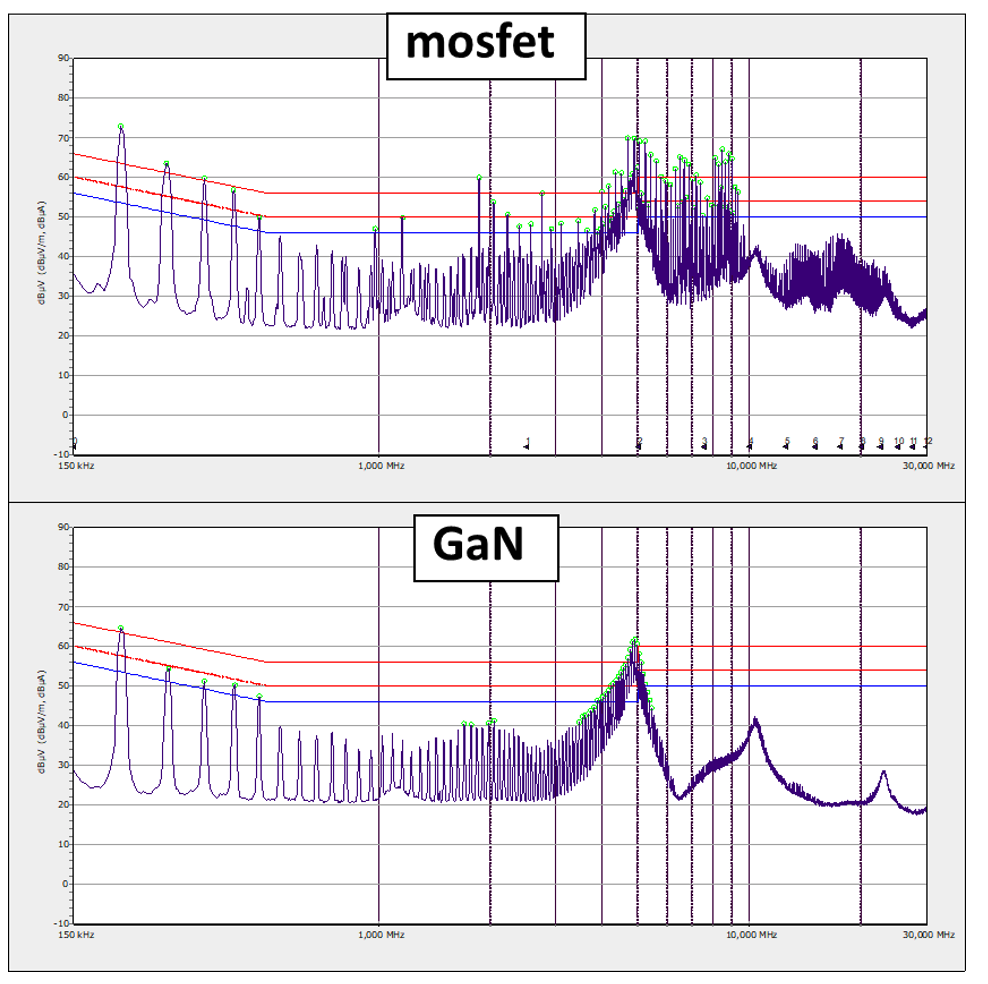
Figure 1 - EMI measurement comparison - GaN v MOSFET (source Buro Springett)
Compared to the initial measurements, the relatively simple task of replacing the MOSFET with a source mounted GaN transistor yielded cleaner emissions 10 dB lower at 170 kHz. Without the switched drain capacitance to the heatsink effect, the GaN transistor eliminated the injected currents to the chassis.
With the primary source of EMI fixed, additional testing revealed other sources of noise, for which minimal cost improvements could be made.
You can read more technical detail about Nigel’s EMI investigations and how by replacing a MOSFET with a Nexperia GaN transistor significantly reduced EMI in the latest edition of Bodos Power.
More information about our GaN FETs, including product datasheets