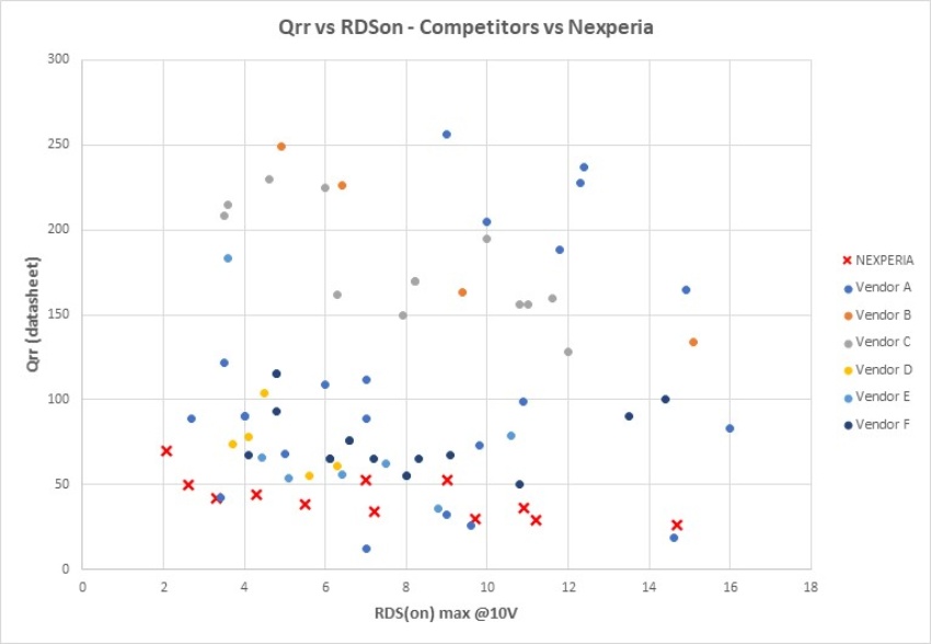
Back in 2018, Nexperia released the first NextPower 100 V MOSFETs with industry leading low Qrr. The recent addition of new 80 V and 100 V devices delivers further improved RDS(on) and enhanced Qrr FOM (figure of merit). With a range of RDS(on) to suit every application and budget, NextPower 80 V and NextPower 100 V MOSFETs are ideally suited for high-performance switching in a range of applications. But why should design engineers care about Qrr and Vsd?
As discussed in Qrr: overlooked and underappreciated in efficiency battle, Qrr can have a significant impact on efficiency and spiking. Yet typically you find Qrr (and Trr) listed at the bottom of the datasheet. Qrr is the amount of charge that accumulates in a MOSFET’s body diode PN junction when it is forward-biased. It takes time to discharge and can result in a significant transient current (Irr), typically a few 10’s of amps for a few 10’s of nanoseconds, resulting in I2R losses in other parts of the circuit. It also interacts with parasitic inductances to create problematic voltage spikes in the drain-source voltage (Vds). Therefore, low Qrr MOSFETs are becoming increasingly important.

The role of the body diode
The MOSFET’s body diode provides a path for inductive load current to by-pass the MOSFET during its “OFF” state. It is therefore an important feature in many applications including synchronous rectification (AC-DC and DC-DC) and motor control (full-bridge & half-bridge). Body diode conduction occurs during the ‘dead-time’ between one MOSFET switching off and the second MOSFET turning on. Although dead-time is typically brief (approximately 80 to 100 nanoseconds) the losses associated with this part of the switching cycle can be significant. There are two main energy loss mechanisms associated with the body-diode conduction phase.
Body diode losses due to Vf
Let’s compare the energy loss due to the body diode’s forward voltage Vf against the energy loss in an ideal 4 mΩ MOSFET over an 80 ns period. Firstly, consider a nominal 20 A load current flowing through an ideal MOSFET, the I2R power dissipation would be 1.6 W and therefore the total energy loss over an 80 ns period would be 0.128 µJ.
Now consider a 20 A load current flowing through a typical body diode with Vf of 1.2 V. Instantaneous power dissipation is 24 Watts. If the dead-time is 80 ns, then energy lost due to body diode’s Vf is 1.92 µJ. Consequently, when current is diverted through the body diode, then energy losses are 15 times higher than the ideal situation. However, by reducing Vf to 1 V, then the energy lost due to body diode’s Vf is 1.6 µJ per switching cycle, or just 12 times higher.
Body diode losses due to Qrr
Again, when we consider an ideal 4 mΩ high-side MOSFET, with a Qrr of 0 nC, then I2R power dissipation would be 1.6 W. So, if the load current flowed continuously for a typical Trr of 40 ns, the energy loss would be 64 nJ.
Then consider an Irr of 20 A with a triangular waveform flowing for the same Trr - the additional power loss in the high-side MOSFET due to Qrr is 32 nJ [((202 x 0.004) x 40 x 10-9) / 2]. So, reducing Qrr by 50% can reduce the energy losses by 16 nJ per switching cycle, helping minimize I2R losses in the high-side MOSFET.
Cutting dead-time
To avoid harmful cross-conduction current (shoot through) between the supply rails, dead-time is required to ensure that both MOSFETs are never turned ON at the same time. It is usually set to provide sufficient time for the MOSFET’s ringing to decay to a safe level. However, low Qrr MOSFETs have a lower peak current and a shorter spike duration. The result is reduced ringing / resonance, which is good for EMI but also gives the design engineer an option to reduce the dead-time. Which further improves efficiency.
LFPAK leads the way
Nexperia’s latest NextPower 80 V / 100 V Low Qrr MOSFETs deliver optimized improvements across the board when it comes to Qrr. Combined with the copper-clip construction of LFPAK, it can further minimize parasitic inductance in the PCB and component lead-frames, and by further reducing Irr that can help reduce the maximum spike voltage by approximately 10 V to 20 V and measured EMI emissions by up to 10 dB in customer’s applications. An improved Vsd (max) of 1 V compared to typical competitive offerings of 1.1 to 1.2 V results in lower body diode losses due to Vf.