Given their fast response times and high efficiency MOSFETs are commonly used as switching devices in a range of applications. And just as choosing the right MOSFET is key, so too is ensuring you have the right MOSFET gate driver. As it directly impacts power efficiency, switching speed, and thermal management in the system. So how do you choose the right MOSFET gate driver for the optimal performance and reliable operation of your design? With the latest addition to our automotive and industrial portfolios, Nexperia helps simplify that choice.
MOSFETs and gate drivers are complementary products for switching solutions. Gate drivers essentially act as the interface between control circuits (like microcontrollers) and the MOSFET gate. Amplifying the logic control signals generated for the timing of the switching process to the necessary voltage and current levels required to accurately switch the MOSFET on and off. For example, a logic device can typically drive loads with approximately 20-50 mA and voltages ranging between 1.2 and 5 V. For transistor gates, gate voltage levels are typically 8-16 V and the peak current drive capability requirements are in the order of several ampere.
Understanding drive capability and switching times
Looking at the basics, the ability to quickly and accurately switch a MOSFET on and off is linked directly to the drive capability of the gate driver. In turn this is dependent on the gate charge (Qg) of the MOSFET. The higher the gate charge, the longer it takes to charge or discharge the capacitor, leading to increased switching losses.
It is relatively easy to calculate the charge time using a gate driver with a given maximum drive capability. For example, using Nexperia’s new NGD4300D high-performance dual MOSFET gate driver, we can work out how long it takes to charge the gate of the 100 V, PSMN2R0-100SSF N-channel MOSFET up to 90%.
From the PSMN2R0-100SSF datasheet we know:
- Total gate charge Qtot of the MOSFET is 160 nC
- Gate capacitance @VGS = 12 V, is Qtot/VCC = 13.33 nF
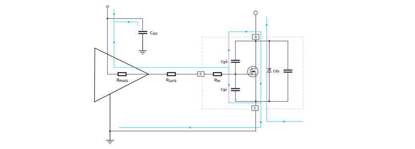
The following figure shows the gate charge scenario, with Cgd and Cgs adding to the total gate capacitance. In our calculation we have neglected additional gate resistance.

The peak drive current of the NGD4300 is 4 A. So, the initial maximum current through the output drive stage is:
- 4A = VCC/Ron => Ron of the output driver transistor = 3 Ω
Voltage drop over the MOSFET of the output stage is:
- VDS = R*I(t) = R*dQ/dt
Voltage drop over the gate capacitance is:
- 1/C * Q(t)
The sum of the voltages in the loop is = 0:
- VCC + R*dQ/dt + 1/C * Q(t) = 0
Therefore, the solution of the first order differential equation is:
- Q(t) = Qtot*(1 – e(-1/RC*t))
- R*C = 3 Ω * 13.33 nF = 40 ns
- Q(t)/Qtot = 0.9 (90% charge) => 1 – e(-1/RC*t) = 0.9 => t = -RC * ln(0.1) = 92 ns.
Switching times and typical half bridge operation
Half-bridge circuits, which are common in power conversion applications, typically operate at frequencies between 20 kHz and 150 kHz. For simplicity if we consider a 100 kHz (10 µs period ) operation, it has a typical dead time of around 150 ns. Even if we assume the maximum operating frequency of a half bridge is 500 kHz, then the period is reduced to 2 µs. With a dead time of approximately 150 ns and rise and fall times of around 92 ns each, stable switching can be assured.
In practice, MOSFET gate capacitance is dynamic, meaning it changes throughout the switching process. As the MOSFET gate charges, it reaches a phase known as the Miller plateau, where the gate voltage temporarily stabilizes while the MOSFET’s conducting channel fully establishes. This phase requires additional charge, resulting in a delay in the charge-up time and effectively slowing down the switching process. However, the calculation above gives a thumb rule estimation about the time we can expect based on MOSFET gate charge and current drive capability of the gate driver.
Nexperia’s NGD4300 brings numerous benefits
The NGD4300 is a high-side / low-side gate driver which is dedicated to switching applications with half bridges driven in alternating switching mode. Rated to 120 V, it is ideal for both main-converted and battery powered applications offering several kW of power.
It has been built on Silicon-on-Insulator (SOI) process technology. This eliminates the parasitic bipolar transistors underneath the complementary NMOS and PMOS FETs, preventing the IC from driving into latch-up.

In addition, the NGD4300 incorporates high-speed logic functions, ensuring excellent delay matching (1 ns typical) is achieved for both low-side and high-side signal paths. As well as delivering superior timing parameters or propagation delay (13ns for both channels).

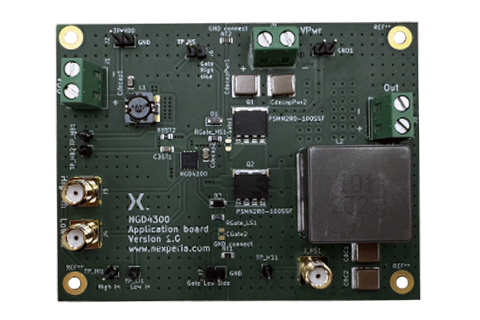
To evaluate the behavior and performance of the NGD4300, you can request the NGD4300 evaluation board and see how effective it is at driving the PSMN2R0-100SSF in a buck converter environment.