Drivers and vehicles now rely more heavily on Advanced Driver Assistance Systems (ADAS). While the use of systems such as RADAR and LiDAR will be important here, ADAS in vehicles also relies heavily on high-quality video imagery. As vehicles become more autonomous, the quality of these video streams will be more important. From a design aspect, high-speed video link design needs to consider how to maintain the signal integrity needed in such a harsh environment.
Some cars already feature systems that can automatically identify road signs or detect when the car is drifting outside of its own lane. These are features that, at least for now, can only be realized using video sensors inside and around the vehicle itself.
Even though the use and importance of video data is increasing in the automotive sector, there are still no globally recognised standards in place to define how the video data should be shared around a vehicle. It is still left up to the manufacturer to choose their preferred solution. This includes proprietary standards such as APIX, GSML and FPD-Link, which support speeds of 6 Gbit/s, 10 Gbit/s and 13 Gbit/s respectively. In addition, the use of automotive-grade Ethernet with speeds of up to 1 Gbit/s is also increasing.
As the demand for bandwidth and resolution increase, the number of video links used in an average vehicle will also build. Standard definition, which only a short while ago was perfectly good for reversing cameras, will be replaced with high definition, high framerate sensors that support high resolution image capture at high traveling speeds.
Maintaining signal integrity is key
From a design aspect, high-speed video link design needs to consider how to maintain the signal integrity needed in such a harsh environment. Every component added to the video data path will introduce losses, this will influence the choice of coaxial cable used, the quality of the connectors and how the signal is routed to the link’s physical interface (PHY). Maintaining signal integrity is paramount but this needs to be balanced with adding suitable levels of protection against potential ESD pulses and fault conditions, such as a short-circuit to the battery rail. The interface also needs to withstand transient voltages of up to 10kV. The impact of the insertion capacitance associated with the protection devices used must be carefully considered in order to provide protection without impacting signal integrity. More details can be found in this white paper.
As an example, the recommendation used to be to place ESD devices as close to the PHY as possible, to protect the IC. This advice has since changed and the preferred position for ESD protection is now to place protection as close to the connector as possible. This will typically mean the ESD device is now on the connector-side of the DC blocking capacitors, as shown in Figure 1. If an optional common-mode choke (CMC) is used, this also means moving the ESD device from the PHY side to the connector side of the CMC.
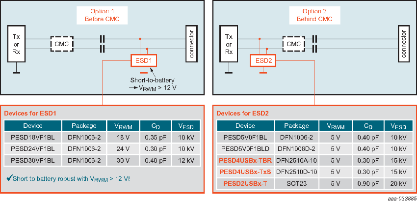.png "Figure 1. Options for ESD placement")
So, why the change of approach? Well, looking at the original position, next to the PHY, it is clear that the ESD device is intended to protect the sensitive electronic circuitry of the PHY. But in order to do that the electrostatic shock would need to pass through the DC blocking capacitors and the CMC. The insertion losses associated with the ESD protection may be minimal in this position, but clearly it leaves other components and parts of the circuitry unprotected.
What is the best position of the ESD protection?
From technical point of view, the best position for the ESD protection is actually as close to the connector as possible. Here, the ESD device can clamp down the ESD pulse to ground while it is still physically distanced from the circuitry and especially the PHY itself. This is the reason why some of the specifications in the automotive sector, such as those proposed by the Open Alliance Special Interest Group (SIG), now recommend that the ESD protection be closer to the point at which the ESD pulse enters the PCB. The intention is to provide ESD protection based on the system’s needs, rather than one specific component. Figure 2 shows how the position of the ESD device has changed.

Moving the ESD device closer to the connector potentially provides protection for more of the circuit, however it has other implications due to its proximity to the connector’s terminals. These implications will shape the design choices made by automotive engineers implementing high-speed interfaces, such as video connections. These choices will relate to the capacitance introduced by the ESD device and how this may impact the rise/fall times of the digital signals present.
Also, because the ESD protection device is now closer to the ‘outside world’ it will be exposed to different threats. This includes a potential fault on the cable that could lead to a short between a signal and a supply rail. In an automotive environment, this means the ESD device needs to be able to withstand a short of at least 12 V across its terminals without failure. If the ESD device were placed behind the CMC and DC blocking capacitors, this requirement is not valid anymore. Figure 1 includes a selection of devices that could be used in either of the two positions, highlighting the different reverse standoff voltage, (VRWM).
Simulations are essential to modern automotive designs
In automotive design, the importance of simulation during a project’s concept phase is becoming essential. Nexperia understands this and supports both the simulation of the ESD event itself and also SI simulation. The evaluation of the ESD protection device can be done using SEED (System Efficient ESD Design) models.
Simulation using the SEED methodology considers the interface along with the rest of the circuit. Models are based on an equivalent circuit to represent the PHY, CMC and blocking capacitors. Both static and dynamic behaviour of the ESD protection can be modelled. Using SEED simulations and models the design engineers can test their ESD circuitry design choices and use the results to help them choose the right ESD protection device, even at the concept phase. Nexperia has used this approach to characterise its ESD protection devices and analyse how they perform against initial and residual currents induced by a controlled electrostatic discharge. Nexperia also provides S-parameter data for all its ESD protection devices, including those used for High-Speed interfaces and especially video links. The S-parameters can be used by design engineers in the SI simulation of their individual system.
Discover more information about Nexperia's ESD products for multimedia bus protection in the automotive industry and to learn more about how SEED models and simulation are used in the protection and SI of high-speed automotive interfaces, check out this useful resource.