It's understood that today’s cars are closer to being electronic gadgets on wheels than the traditional vehicles most of us grew up with – and while we once marvelled at the inner workings and the sense of control by peeking under the hood, the evolution of modern cars has transformed them into complex computers. The relentless electrification we have seen in recent years continues to extend throughout the vehicle, as designers seek to save weight, improve reliability, ease vehicle assembly, create differentiating features, and implement advanced driver assistance and automated driving systems. Not to mention what’s happening with the drivetrain.
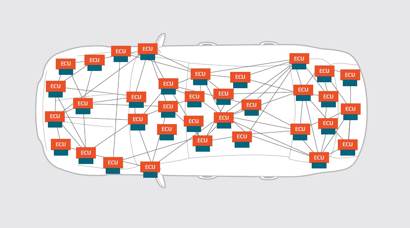
At the beginning of the trend, when electrification was confined to certain vehicle functions, a domain-based approach to control made perfect sense. However, as the amount of software increased and the risk of software malfunction grew, the demand for software upgradeable units became evident. The complexity arising from a wide variety of ECU combinations further intensified the challenges, making it nearly impossible to implement effective upgrades. This led to the integration of numerous electronic control units (ECUs) to handle the expanding functionality, resulting in some vehicles containing over 100 of these modules. They all needed to be installed somewhere in the vehicle’s structure, although space was severely limited. Wiring also became complex and heavy, running counter to the ideals of saving weight and improving reliability.
Today the increasing feature sets of cars are being bundled among dedicated ECUs. This zonal architecture is favoured today and enables the numbers of ECUs to be reduced and permits simplified wiring. Such a “frozen” feature set can mean cost reduction. But, as with any engineering challenge, achieving gains in one area calls for giving back in another. Consolidating multiple different functions in the smaller numbers of ECUs can mean these units become excessively large, heavy, and power-hungry. A compromise we shouldn’t have to accept!
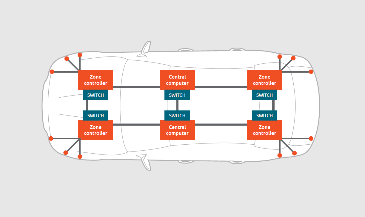
Development from distributed to modern zonal E/E architecture in automotive.
Power Semiconductors in Vehicle Infrastructure
Engineers and designers are already meeting this challenge with the venerable techniques of the electronics industry: increased semiconductor integration and more complex, multi-layer substrates, allowing for closer component spacing and thus smaller PCB sizes and smaller box dimensions.
However, with all this extra circuitry on board also comes an increase in the typical power demand of each ECU. The squeeze on space necessitates power supply circuitry to become smaller, while handling more power at the same time. This drives up power density and demands increased thermal dissipation to prevent overheating and early ECU failure.
In other industries, designers have quickly adopted advanced power-conversion topologies using techniques like synchronous rectification and zero-voltage switching to raise efficiency and reduce dissipation. In automotive, however, factors such as cost, reliability, and ruggedness take precedence and tend to steer designers towards more conservative, proven topologies like asynchronous buck, boost, and SEPIC converters. So, while the pressure on power density pushes component vendors to develop packages with a smaller footprint, the components must dissipate the same amount of heat.
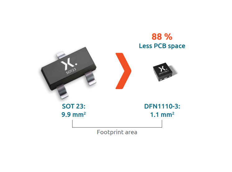
New semiconductor packages are needed for transistors and rectifier diodes, that are both space-saving and extremely thermally efficient. For many product generations, designers have relied on established packages like SOT23 and SMx (SMA, SMB, SMC). However, with rapidly evolving requirements, there is now a pressing need for new packages that offer superior heat dissipation capabilities.
Innovation Under the Skin: How modern packages master efficient heat dissipation
But what are the modern packages up against? SOT23 is one of the most popular surface-mount packages for transistors and diodes used across all industries. This leaded package, in which the die is attached to a lead frame, often directly to the source terminal while bond wires attach the gate and drain leads, offers a few points to improve upon. On the other hand, DFN (discrete flat no-lead) devices have – as the name suggests – no leads. Instead, it features a dual row of terminals on the underside which are closely spaced, allowing for shorter bond wires.
These shorter bond wires also enhance electrical performance by lowering package inductance, die-free package resistance (DFPR) and thermal resistance. In the established SOT23, internally generated heat must travel through the die-attached layer to the lead frame and along the source lead until it reaches the substrate. In contrast, the more modern DFN conducts heat from the die directly downwards to the source pad on the package underside: a much shorter journey that ensures more efficient heat dissipation.
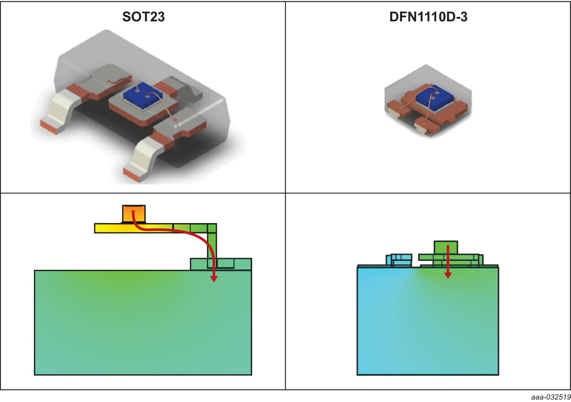
Inside view and heat dissipation path of SOT23 and a DFN package
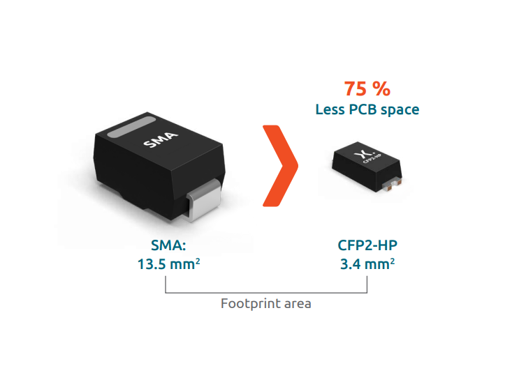
Designers of power circuits are also looking for improved heat dissipation from power diodes, as these can carry a significant current during switching transitions. The SMx packages, which have been the designer’s choice for many years, are now giving way to newer packages like Clip-bonded FlatPower (CFP) type. While saving 38-75% of PCB area compared to an SMx of similar rating, CFP packages have equal or better power-handling capability. That’s a significant boost in dissipation capability, when expressed as W/cm².
Much of the performance improvement achieved with CFP packages is due to the copper-clip technology which we created as an alternative to conventional wire bonding. It has now been more than 20 years since we first introduced the loss-free package, LFPAK, that brought this technology to the market. An innovation of such magnitude, it caused disbelief among experienced circuit designers that such a tiny package could deliver such a high power-handling capability. The key is the copper clip, which enhances cooling from the die topside as well as the underside. The top-side attachment has a greatly enlarged surface area compared to an ordinary bond wire attachment and a much shorter dissipation path from silicon to the PCB, while the clip’s large cross-sectional area ensures efficient thermal conduction through to the underside of the package and into the substrate.
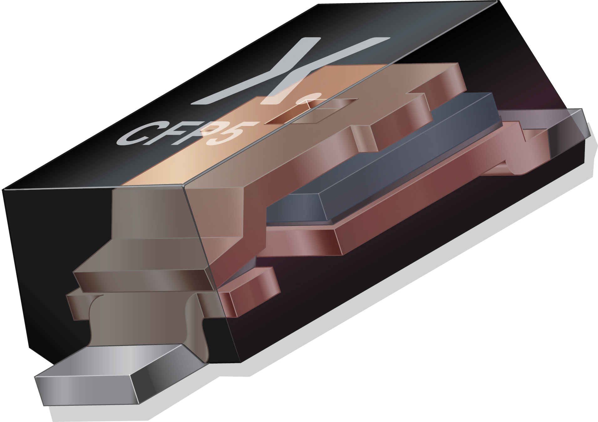
Inside view of a clip-bonded package (CFP)
Small size, big impact: CFP and DFN win on price and performance
The demand for smaller footprint with high thermal efficiency is now prevalent throughout automotive applications, including LED lighting systems, the traction inverter, the battery-management system (BMS), and the high-power on-board charger (OBC). At Nexperia, we believe that CFP will be the power-diode package of choice in the future just as DFN will be for small signal diodes and transistors. This transition is happening right now. We are already investing to increase manufacturing capacity.
The new package style is needed urgently. The increasing computing power in a modern car also requires high pin count MCUs, making multi-layer PCBs a prerequisite for proper wiring. The cost of these PCBs justifies the usage of smaller footprint packages that offer the same electrical performance. Even if a smaller package solution comes with a higher part cost, the reduced system cost justifies the adoption of CFP and DFN packages.
However, in many cases reduced part cost is already inherent to smaller packages. These packages are being produced more cost-effectively on modern package assembly lines as the package cost scales with the package size. We see that CFP packages are outperforming traditional package outlines such as SMx, DPAK, TOx when it comes to production cost. Something we predict will also happen to DFN packages.
The relentlessly growing demands of modern automotive and industrial applications are already driving a trend in the components market that is affecting price and availability. Demand is set to outstrip the capacity and availability of the “legacy” packages such as SMA, SMB and SMC, which will force designers to adopt the better performing alternative if they are to future-proof their products.
Summary
Today’s demands for smaller, more powerful, and more reliable automotive ECUs echo calls coming from almost all markets for electronic products. But the good news is: this is made possible by the latest developments in efficient packaging, which drastically reduce the footprint of power transistors and power diodes while promoting cooling.
Nexperia continues to invest heavily in expanding its capacity to match the growing market demand, especially in automotive and industrial applications, for CFP- and DFN-packaged products. By bringing multiple versions of these devices to the market we underscore our commitment to expanded manufacturing capacity and accelerated transition to smaller, thermally optimized packages.
Discover how you can save PCB space and future-proof your design with Nexperia's CFP and DFN packages for the diodes and transistors in your design nexperia.com/save-pcb-space