The maximum data rate of USB4™ is 40 Gbps, utilizing all transmit (Tx) and receive (Rx) lines offered by the USB Type-C® cable. This means 20 Gbps for each differential line pair, corresponding to a signal fundamental frequency of 10 GHz for each differential line pair. While the RF performance of ESD protection devices is traditionally compared by looking at their electrical capacitances, this method reaches its limit at around 10 GHz. As the capacitance and inherent inductance of an ESD protection device are effectively forming a band-stop filter.

Looking into the structure of an ESD protection device, its parasitics can be split into the capacitance (main contribution comes from the protection diode), inductance (main contribution comes from the package bondwire) and resistance.
To emphasize the importance of the inductance of the protection device, Nexperia compared the measured insertion loss behaviour (solid line) of a wire-bonded ESD protection device to a calculated insertion loss curve (dashed line) of an ideal capacitance C of the same value @ 10 GHz as the measured device. The deviation at 10 GHz due to the wire-bond inductance is notable.
It is obvious that the capacitance alone does not describe the behaviour of the device at frequencies of 10 GHz and higher. The band-stop resonance frequency  of the protection device is clearly visible. For frequencies in the GHz range, S-Parameters should be used rather than capacitances to assess the RF suitability of ESD protection devices.
 with the measured insertion loss of a wire-bonded device having the same capacitance at 10 GHz (solid line).")
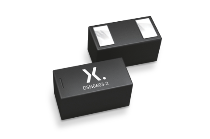%20package%20.png "Nexperia’s SOD962-2 (DSN0603-2) is an example of a monolithic Silicon package optimized for low inductance. The narrow solder pads support system designs with low return loss.")
As a consequence, the suitability of ESD protection devices for USB4 data rates should be rated through S-parameters, notably |S21|(insertion loss or αIL) and |S11| (return loss or αRL) to describe the additional attenuation and reflection of the signal due to the ESD protection device. It should be noted that S-parameters are measured on 50-Ohm single-ended systems (100 Ohms differential), since this is the standard for measurement equipment, while USB4 data lines typically have line impedances of 90-80 Ohms differential (45-40 Ohms single-ended).
How package design supports RF performance of ESD protection
Thus, an ESD protection device with a lower inductance will offer a better RF performance when compared to another device with the same capacitance but higher inductance. On top, a lower inductance to GND allows a faster reaction of the ESD protection device, resulting in a lower clamping for fast transients such as ESD pulses. For both reasons, bondwire-less monolithic Silicon packages are preferred for ESD protection of very fast data lines. A package with narrow solder pads supports system designs with low return-loss.
Insertion loss and return loss budgets for USB3.2 and USB4 systems
An overview over Host/Device insertion loss budgets can be seen below for orientation. The host/device budget for USB4 Gen 2 (10 Gbps) is smaller compared to USB4 Gen 3 (20 Gbps) to allow a larger budget for longer cables up to 2m.
|
|
Host / Device budget |
frequency |
|
USB3.2 Gen2 (10 Gbps) |
8.5 dB |
5 GHz |
|
USB4 Gen 2 (10 Gbps) |
5.5 dB |
5 GHz |
|
USB4 Gen 3 (20 Gbps) |
7.5 dB |
10 GHz |
While it might look desirable to choose an ESD protection device having insertion loss and return loss as small as possible – and Nexperia can offer down to -0.19 dB insertion loss and -23.5 dB return loss @ 10 GHz, if required – there is a balance between RF- and clamping-performance: Improving RF performance in the same technology will reduce the clamping performance. It will also reduce the robustness of the ESD protection device but for high data-rate transceiver ICs, we have experienced that this transceiver IC is typically damaged due to the remaining clamping before the ESD protection device is damaged due to ESD overstress.
Nexperia have just released a new product family optimized for very fast data lines, offering these RF performances:
|
|
αIL @ 10 GHz, |
αRL @ 10 GHz, |
|
-0.19 |
-23.5 |
|
|
-0.25 |
-19.4 |
|
|
-0.28 |
-19.0 |