Our copper clip technology boosts power handling, electrical efficiency, and reliability – making it ideal for the incoming generation of wide-bandgap devices.
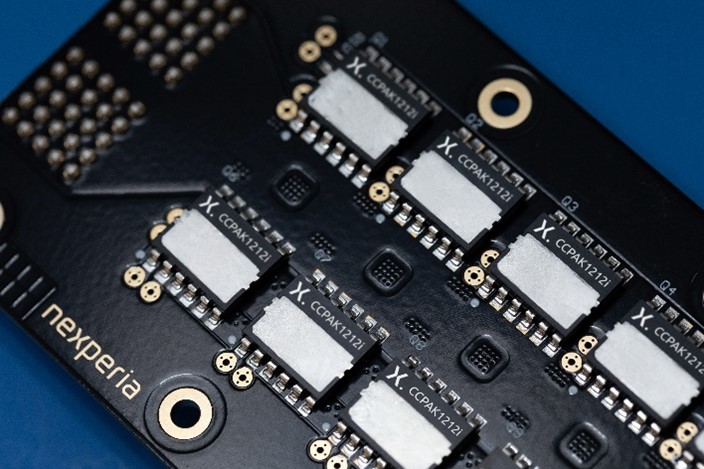
Nexperia’s copper-clip technology has been a game changer for power packaging and continues to set the pace in performance and efficiency. Around 90% of our product range now uses the LFPAK loss-free package that introduced copper clip back in 2002, and this technology features prominently in the new CCPAK1212 that houses our latest GaN FETs.
We developed the LFPAK to meet the computing industry’s need for extremely high current when powering the latest processors. As each new silicon technology node brought exponentially more transistors on-chip, while also lowering the supply voltage, the peak current began heading towards 200 A and beyond. This stretched the capabilities of the industry-reference SO-8 transistor package, driving power supply designs towards larger packages such as DPAK and even D2PAK to handle it all.
We developed the LFPAK56 to deliver more power from the popular SO-8 package footprint, so that the LFPAK56 could be used instead of DPAK or D2PAK. Our first generation of 25 V MOSFETs in LFPAK56 (named after its dimensions – 5 mm x 6 mm) had RDS(on) and maximum drain current comparable to similar devices in DPAK, despite having a footprint less than half the size: 30 mm2, versus the DPAK’s 70 mm2. The copper clip attachment, which replaces traditional bondwire connections between the die and leadframe, has a huge cross-sectional area and so delivers a vast increase in both electrical and thermal performance.

At first, the industry was sceptical: how could this LFPAK56, less than half the size of a DPAK, achieve equivalent thermal performance? Some doubted the reliability of the clip attachment, although the physics was beyond doubt: soldering the clip directly to the source connection on the die eliminates the areas of high current density that normally occur where bond wires are attached. Thus, copper clip prevents the formation of temperature “hotspots” at these locations and so protects the transistor.
Reliability and thermal performance testing duly showed that the LFPAK could perform as claimed. LFPAK56 has also passed the stringent AEC-Q101 automotive qualification and, in fact, significantly exceeded every requirement.
The copper clip also reduces package inductance, which is three times lower than that of conventional wirebonded packages and thus permits better switching efficiency and lower EMI. Boosting switching efficiency is increasingly important in today’s power supply designs, which target higher frequencies to realize greater power density and faster dynamic response. It’s why our latest copper clip package, the CCPAK1212, is such a great choice for our new GaN power transistors. Their wide-bandgap technology delivers excellent efficiency in fast-switching designs, making GaN and copper clip a perfect pairing.

We shipped more than 1.7 billion LFPAK devices in 2021, including MOSFETs and bipolar power transistors in LFPAK56 and its later derivatives from small size of 3 mm x 3 mm LFPAK33 to 8 mm x 8 mm LFPAK88. With the new CCPAK1212 now adding to the copper clip success story, we expect this technology to feature prominently in advanced power semiconductors for generations to come, either using GaN, SiC or MOSFETs devices.