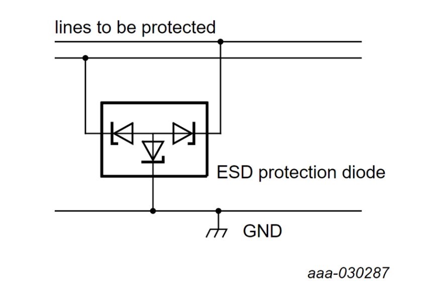
If we consider the ideal ESD protection device, it does not impact signal integrity while clamping all overvoltage transients to keep the protected system in its Safe Operating Area. It will also not need additional space or routing.
When looking for the 'ideal' ESD protection solution for high-speed lines, there are a three main challenges - signal integrirty, system-level ESD robustness and footprint. Addressing signal integrity, we need an ESD protection device with low capacitance but also low inductance, which is quite often overlooked. While from a system-level ESD robustness perspective, a low clamping voltage is becoming more important than robustness of the ESD protection device itself. Although surge robustness of the protection device has once again become important due to potential fault conditions, where data lines might be shorted with supply lines. Nexperia addresses both these challenges by using advanced TrEOS silicon technology and advanced packages derived from Wafer-Level Chip-Scale Packaging (WL-CSP) technology.
But what is the best way to reduce the footprint demand of ESD protection? An obvious approach is by simply shrinking the package size. Metric 0603 packages (0201”) are now the accepted standard for the mobile industry and are rapidly becoming the standard in computing.
The smaller 0402 metric (01005”) is already being used in applications where space demand is most stringent. And due to the RF demands of USB4 data lines and parameters like Return Loss becoming important, with narrower solder pads a move from 0603 to 0402 will offer lower Return Loss when comparing the same diodes in this package. However, these smaller packages does placing higher demands on assembly technologies.
Doubling protection within the same footprint
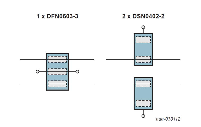
An alternative approach is to take the existing 0603 (0201”) footprint and use it to protect two lines, a differential line pair, by creating a 2-in-1 solution in Nexperia’s new DFN0603-3 (SOT8013) package.

The DFN0603-3 concept allows several advantages:
- 2-in-1 approach means two protection devices but the footprint of one
- A differential line pair can be protected with virtually no additional space demand.
- Having two ESD protection devices on one monolithic chip offers extremely high symmetry, supporting very good signal integrity on differential data lines.
- Smaller solder pads introduce less Return Loss to the system.
- DFN0603-3 is an industry-standard footprint
Nexperia have taken this DFN0603-3 package and added TrEOS ESD protection to it. Which depending on needs, means the product family offers capacitance down to 0.2 pF, surge robustness up to 11 A and clamping of a 4.4 V @ 8 A 8/20 µs surge.

Added RF performance
So we get very high robustness and very low clamping. But what about the RF performance? From the application side, we recommend strongly to connect the middle pin to GND – the device is designed to protect very fast differential data lines, so the protection should be as symmetrical as possible.
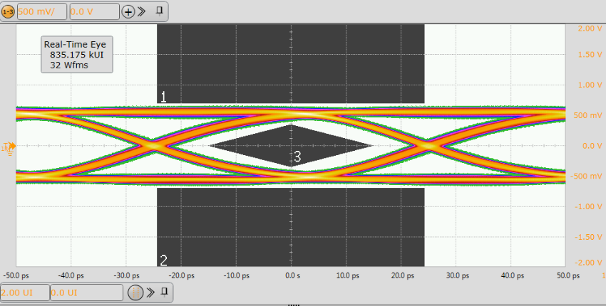
Taking a quick look at a 20 Gbps Thunderbolt eye diagram of a PUSB3BB2DF mounted at a test board (the board has not been de-embedded), we already see the potential of the new DFN0603-3 package for outstanding RF performance.

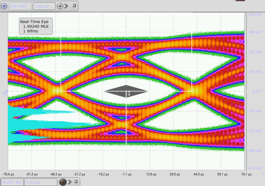
Since the device is also HDMI capable, we tested the performance of the PUSB3BB2DF with an HDMI2.1 eye diagram - 12 Gbps FRL, 8dB, and to make things more interesting, Worst Cable Model 3. Again, the test board was not de-embedded and the DFN0603-3 shows excellent RF performance when protecting very fast data lines.

Proven protection that saves space
Nexperia’s new DFN0603-3 package offers a 2-in-1 solution, where two ESD protection devices are provided in the same footprint as one. Keeping the benefits of TrEOS technology, very low capacitance, very low clamping and very high robustness, and also showing outstanding RF performance on very fast data lines.
An Application note showing our Recommendations for Printed Circuit Board assembly of DFN0603-3 is available.