With greater system complexity and ever-increasing sensitivity, it is vital to understand what good ESD protection looks like and how to choose the right ESD protection device – fit for the system and its application.
It’s not enough that an electronic system performs correctly, it must continue to do so in a safe manner under all conditions the application might face. Therefore, great care must be taken to safeguard the system against interruption or damage by ESD strikes.
From a system perspective, we can help minimize any potential ESD impact by carefully managing the overall system design. For example, we can start by ensuring we place sensitive and vital circuits away from the perimeter of the circuit board. Aim to use the shortest electrical path to the protection device and avoid parasitic inductances. And as incoming surge energy is dissipated in the protection device, placing low-capacitance ESD protection as close as possible to the external I/O ports is important.
We also want the protection device to be effectively invisible to the system during normal operation. Deterioration of the data channel’s bandwidth should be minimized - eye diagrams should to be kept open. Yet the protection device needs to instantly react to shunt dangerous current and voltage spikes to ground during surge and ESD events.
How to protect the device – first things first
Understanding where a strike is likely to come from is only the beginning. Will it be from human contact (Human Body Model), other equipment (Machine Model) or from the normal use of the device (Charged Device Model)? Answering this will give an idea as to what level of protection the device needs.
The next question to ask ourselves is about what we’re aiming to protect. Interfaces are especially susceptible to ESD damage and EMI interference but, for most of them, external ESD protection devices will offer a decent protection. Very fast transceiver SoCs on the contrary need highly advanced ESD protection devices to achieve the targeted IEC ESD robustness. And today’s interfaces which combine power and data capabilities, like USB Type-C, require even more care when choosing protection (because we also need to consider leakage or short circuit scenarios between data lines and the supply line VBUS).
System-level robustness –the weakest link
We often hear that system level robustness is directly linked to the robustness of individual components. In practice, it depends on several factors.The robustness of the weakest system-relevant device (usually the SoC) is key. But so too is the protection device’s properties – for instance it’s capability to clamp the surge voltage low enough to let the SoC survive, yet still react fast enough and withstand many ESD events during its lifetime. Other important factors include the PCB layout, the ohmic resistance of wires and any capacitive / inductive parasitic components.

For good system-level robustness, picking the right ESD protection is essential to achieve a minimized residual voltage at the system IC I/O-pin during an ESD strike or other surge event. Low capacitance specifications and an RF-compliant routing concept will minimize the influence on signal integrity. The more sensitive the port pins of the SoC, the more effective the protection should be.
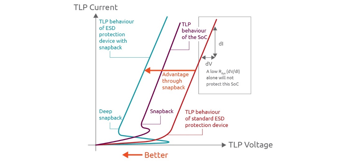
To combine low capacitance with an extremely low clamping voltage for ESD pulses, advanced devices offer active snap-back behavior when triggered by ESD. Such devices have a high impedance in normal operation but switch into a low impedance condition after being triggered. Following an ESD event, they will turn off again so that normal data communication can continue.
Dynamic resistance is an important device parameter for protection devices. A low value means that clamping voltage increases just slightly when the device has to shunt higher current.
Getting the right characteristics
Choosing the right ESD protection device is helped by understanding the device’s key parameters on the datasheet, especially the ‘limiting values’. Among them, the standoff voltage VRWM indicates the maximum operating voltage range for which leakage current is below a specified value IRM. For an indication of the device’s robustness, also check IPPM which is the maximum surge current that a device can withstand if an IEC61000-4-5 pulse with an 8/20 µs timing is applied.

While the device’s breakdown voltage VBR is important, with snapback devices this parameter can be misleading. Other characteristics to look out for include diode capacitance Cd which is related to a signal line’s maximum frequency. When protecting interfaces, VCL clamping voltages are key too, for IEC61000-4-5 pulses at different peak currents Ipp. Last but not least, look for lower value dynamic resistance Rdyn for better clamping performance and monitor TLP curves which show the clamping capability for high-speed pulses like ESD.
To get a deeper understanding, check out our ESD Application Handbook which provides an in-depth exploration of all the facets of ESD characteristics, design, testing and topologies.