Bipolar junction transistors (BJT) are turned on and off using base current. However, because the voltage drop across the base-emitter diode is highly temperature-dependent, in many applications, a series resistor is required to maintain the base current at the desired level to ensure stable and safe operation of the BJT. Discover how RETs can be used to overcome the temperature dependence of standard BJTs.
To reduce component count and simplify board design, Resistor-Equipped Transistors combine single or dual bipolar transistors with the bias resistors and are integrated on the same die. Alternatives include a second integrated resistor parallel to the base-emitter path to create a voltage divider that sets the base voltage. This offers finer tuning and better turn-off characteristic behaviour. Since these internal resistors have higher tolerances than external resistors, RETs are suitable for switching applications where the transistor operates in an on- or off-state. This is why RETs are sometimes referred to as digital transistors. This article discusses some critical operating parameters when designing with RETs in switching applications.
")
Voltage and Current (VI) parameters
The current gain hFE of a RET is defined as IC/IIN, where IIN includes the base current and the current flowing through R2 (where IR2 = VBE/R2). Because of this, hFE is smaller compared to RETs, which have a series base resistor R1 only. hFE becomes smaller for lower values of R2 because the input current is diverted away from the base. This fact can be seen in Table 1. VCEsat is the residual collector-emitter voltage in a RET switch when it is in the on-state.
 and VI(off) dependency on resistor configuration R1/R2 for Nexperia’s NHDTC RETs")
The test condition for measuring hFE is to apply a 0.5 mA base current and 10 mA collector current. VI(off) is the input voltage at which a RET device turns off. This is the condition where the collector leakage current is 100 µA for a collector-emitter voltage (VCE) of 5 V. The lower value provided in the table as V(Ioff)max is considered the maximum allowed output level of the stage driving the RET. This condition must be met to ensure the safe operation of the RET in the off-state. When testing a RET in the on-state, VI(on)min is the most critical parameter. The circuit driving the RET must be able to provide this level of voltage to ensure a safe turn-on. The on-state is defined as the condition where a collector current of 10 mA flows when the collector-emitter voltage is 0.3 V. The VI rating stated in RET datasheets is valid for these test conditions only. RETs require a bigger base drive voltage VI(on) for larger switching currents. Figure 2 shows a RET transistor's Voltage-Current (VI) switching characteristics.
- VI < VI(off)max: All RET devices are guaranteed to be in the off-state
- VI < VI(off)typ: a typical RET is in the off-state
- VI > VI(on)typ: a typical RET is in the on-state
- VI > VI(on)min: All RET devices are guaranteed to be in the on-state
Table 1 shows the dependency of the on- and off-state input voltages on the resistor divider configuration in Nexperia’s NHDTC series of RETs. In the VI(off) condition, a tiny base current flows in the transistor (about 0.3 µA). The typical voltage required to turn off a RET relates to the resistor ratio R1/R2. When the transistor is turned off, this can be calculated with a voltage drop target across R2 or the base-emitter diode. For the NHDTC series, this voltage is approximately 580 mV. Therefore VI(off) values for a resistor ratio of 1 have the same voltage (rows 1-3 in Table 1). The typical off-state voltages when R2 is 47 kΩ with different values of R1 (2.2 kΩ, 4.7 kΩ, and 10 kΩ) are lower for the reasons previously considered. For VI(off) max, even values are stated to ensure that devices operate in the dark green shaded area on the very left area of the graph shown in Figure 2 above.
Nexperia's RET portfolio
The proper selection of the resistor divider is essential so that the control voltage window of the RET is appropriate to the driving stage. The desired collector or load current impacts the base current to be provided for the on-state. A higher collector current can be set using a lower value for R1 and/or less bypass current through R2.
Apart from generic families, Nexperia also provides RET devices with enhanced features, like, for example, the NHDTA/NHDTC series of RETs (see Table 1 above), with a VCEO of 80 V. This feature makes these devices ideal for use in 48 V automotive applications. The PDTB and PBRN families of RETs support collector currents of 500/600 mA and can be used to switch power relays and power LEDs.
Temperature considerations
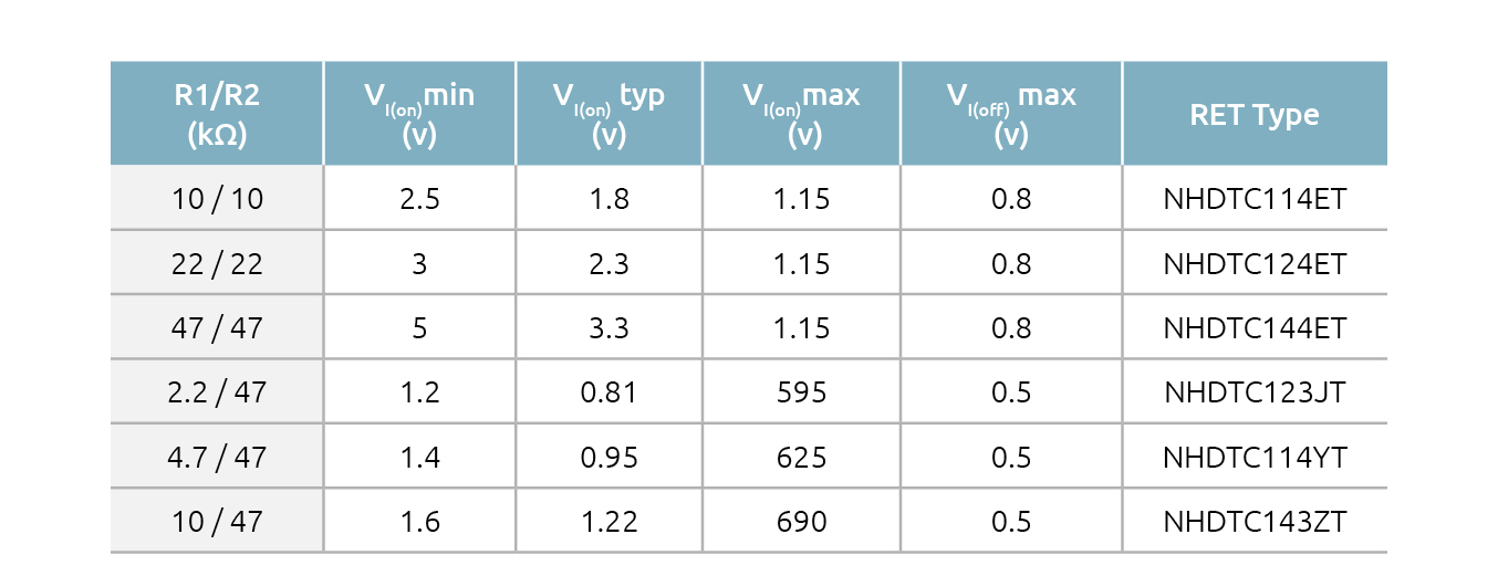
In a practical application, the temperature drift of the VI parameters requires careful attention. The VBE of BJTs decreases as temperature increases, with a coefficient of approximately -1.7 mV/K to -2.1 mV/K. hFE also increases by about 1% per Kelvin for a stand-alone BJT, as shown in Figure 3.
Typical DC current gain as a function of collector current
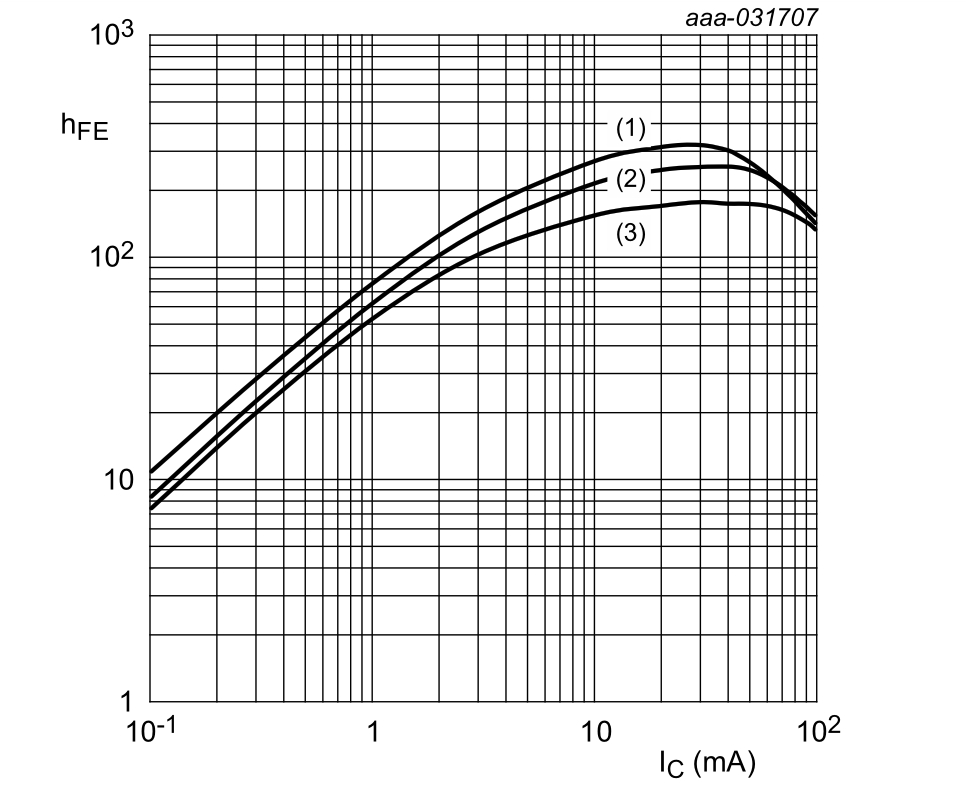
VI(on) is shown as a function of IC, so a higher input voltage is required to drive more collector current at the same VCE. A low ambient temperature requires higher input voltage because VBE increases and hFE drops. Therefore turning on a RET switch at low temperature is the most critical operating condition for an application and requires sufficient input voltage to turn on a device properly (Figure 4).
Typical on-state input voltage as a function of collector current
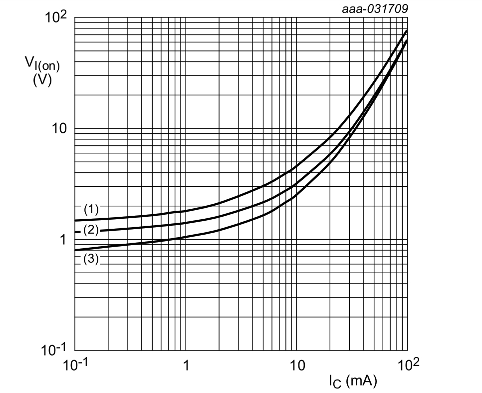
In the off-state, a high-temperature condition is the most critical scenario. Hence, the driver circuit has to be designed to output a voltage well below the typical VI(off) for the highest application temperature (Figure 5).
Typical on-state input voltage as a function of collector current
Simple, yet safe and reliable
RETs are relatively simple devices that are suitable for use in switching applications. Nonetheless, designers must understand the parameters that affect their operation, including switching voltages and currents and how they are affected by temperature. This blog article has provided design tips to ensure Nexperia’s RETs operate safely and reliably in their intended application.