Choosing a low RDS(on) MOSFET for an efficient low loss power switching application? Don’t forget to check there are no hidden compromises.
Power-hungry applications are demanding improved system efficiencies to meet consumer and regulatory requirements for cleaner air and reduced carbon footprint. This is driving the demand towards the ideal 'loss-less' power switch, and in most modern electronic systems this switch is realised with a power MOSFET.
The perfect power switch would have infinite resistance when turned off, zero resistance when turned on and the transition between off and on would be instantaneous, without causing spikes or other transient noise. However, in the real world of MOSFETs, the resistance when turned off is finite, there will always be some leakage current (IDSS), and as hard as semiconductor manufacturers try, the resistance when turned on (RDS(on)) will never be zero. But that does not stop them trying to get as low as possible.
Various methods of reducing the RDS(on) of trench MOSFETs can be used, each of which can have unwanted side effects that affect performance in various applications.
For a typical power MOSFET, the ‘active’ part of the trench structure is contained within the top few µm of the silicon, most of the losses occur within this region. The remaining silicon, known as the substrate, provides mechanical stability during the manufacturing process. Reducing the substrate thickness can significantly reduce the MOSFET’s electrical & thermal resistance, but back-grinding can incur additional costs.
Cell pitch
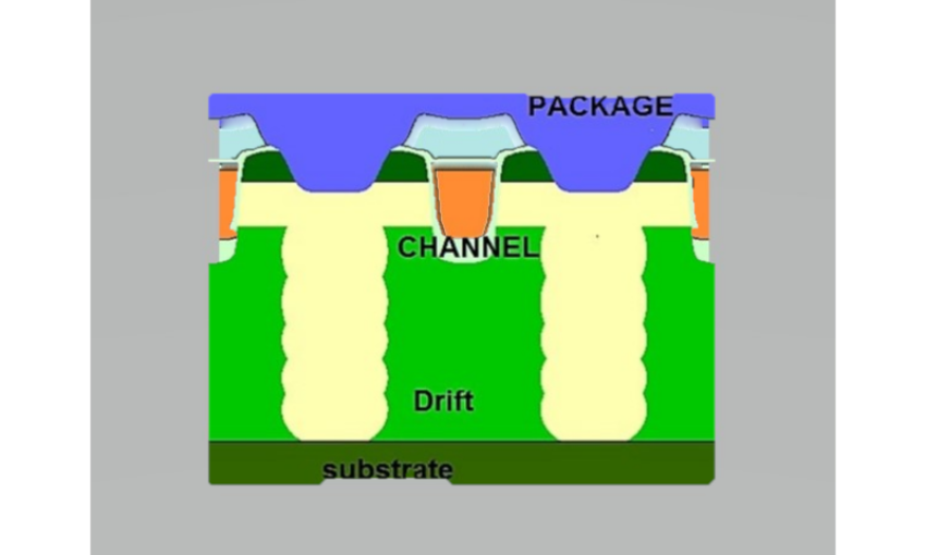
Lower RDS(on) is generally achieved by most vendors by adding more parallel channels, this usually reduces the cell pitch which can cause thermal instability as adjacent cells cause temperature rise affecting the threshold voltages of the channels. It also increases the capacitances of the MOSFET affecting the switching performance. In contrast, SOA may be compromised significantly with narrow cell pitch. Superjunction technology using deeper trenches with P type pillars can reduce channel resistance without reducing the cell pitch, and without affecting the SOA performance.
Drift resistance, by changing the doping of the drift region the RDS(on) can be reduced but the IDSS leakage current and VDS voltage rating in the off condition may be negatively affected. IDSS is often used a manufacturing final test to screen out defective devices, accepting higher leakage current can mean that more defective products may go undetected during final test

Package resistance
By using copper clip and drain pad to replace bond-wires, the package resistance can be reduced, combined with the use of multiple source pins then there will also be a positive effect on inductance, current rating, thermal performance and robustness throughout the life of the product.
It goes without saying that reducing the RDS(on) can sometimes lead to unwanted trade-offs, demanding applications such as power ORing, hotswap, motor drives and load switching may not be able to accept these trade-offs - And nor should they.
NextPowerS3 MOSFETs – Superfast switching with soft-recovery
Nexperia’s latest addition to the NextPowerS3 portfolio combine superjunction technology with copper-clip LFPAK package to deliver competitive RDS(on) to the market. The latest parts provide 0.5 mΩ (typical), up to 380 A DC current rating, in addition to 6x the linear mode (SOA) performance (see diagram below) and competitive Qg / RDS(on) figure of merit.
The new parts give improved performance without compromising other vital parameters.
Latest products
|
Device |
VDS [max] (V) |
ID [Max] (A) |
Tj [Max] (˚C) |
RDS(on) [max] @ 10 V (mΩ) |
|
30 |
380 |
175 |
0.67 |
|
|
30 |
300 |
175 |
0.82 |
|
|
30 |
160 |
175 |
1.9 |